Prof. Satinder Kumar Sharma
| Designation: | Professor |
|---|---|
| School of Computing & Electrical Engineering (SCEE) | |
| Room-217, First Floor, A-4 Building, | |
| Indian Institute of Technology (IIT) Mandi | |
| South Campus, Mandi, H.P., India-175075 | |
| E-Mail: | satinder@iitmandi.ac.in |
| Office Phone: | 01905-267841 |
| Research Group: | Device Engineering Lab (DEL) Group |
| ORCiD: | 0000-0001-9313-5550 |
| Web of Science: | B-4006-2013 |
| Research Gate: | https://www.researchgate.net/profile/Satinder_Sharma |
Additional Responsibility
- Head, International Relations Division (IRD)
A9-Building, 4th Floor, North Campus,
Indian Institute of Technology (IIT)-Mandi
MANDI, H.P., India-175075
Email: headird@iitmandi.ac.in
Research Interests
-
VLSI Technology
CMOS Device Fabrication & Characterization
CMOS Memories, FETs and Logic Devices
Advanced Next Generation Lithography
Nano/Micro Fabrication & Design
MEMS,NEMS, Sensors
Optoelectronic, Photovoltaic & Self-assembly
Microelectronics Circuits & System
List of Patents Granted & Filed:
Patents Granted:
-
Process Development for Epitexial Grown Germaniumn FinFETs Intergrated on Cost Effective Silicon
Platform
Inventors: Sumit Choudhary, Satinder K. Sharma, Jorg Sculze. (Application number: 202311061662)
- Reconfigurable Reduced Switching Activity (Rsw) Mode For An Analog-To-Digital Converter.
Inventors: Ashish Shirish Joshi, Hitesh Shrimali, Satinder K. Sharma. (Application number: 201911042977)

- A Novel Bifacial Perovskite Photovoltaic Architecture for Harvesting Energy form Artificial Indoor
LED Light Sources.
Inventors: Ranbir Singh, Satinder K. Sharma. (Application number: 202211063783)

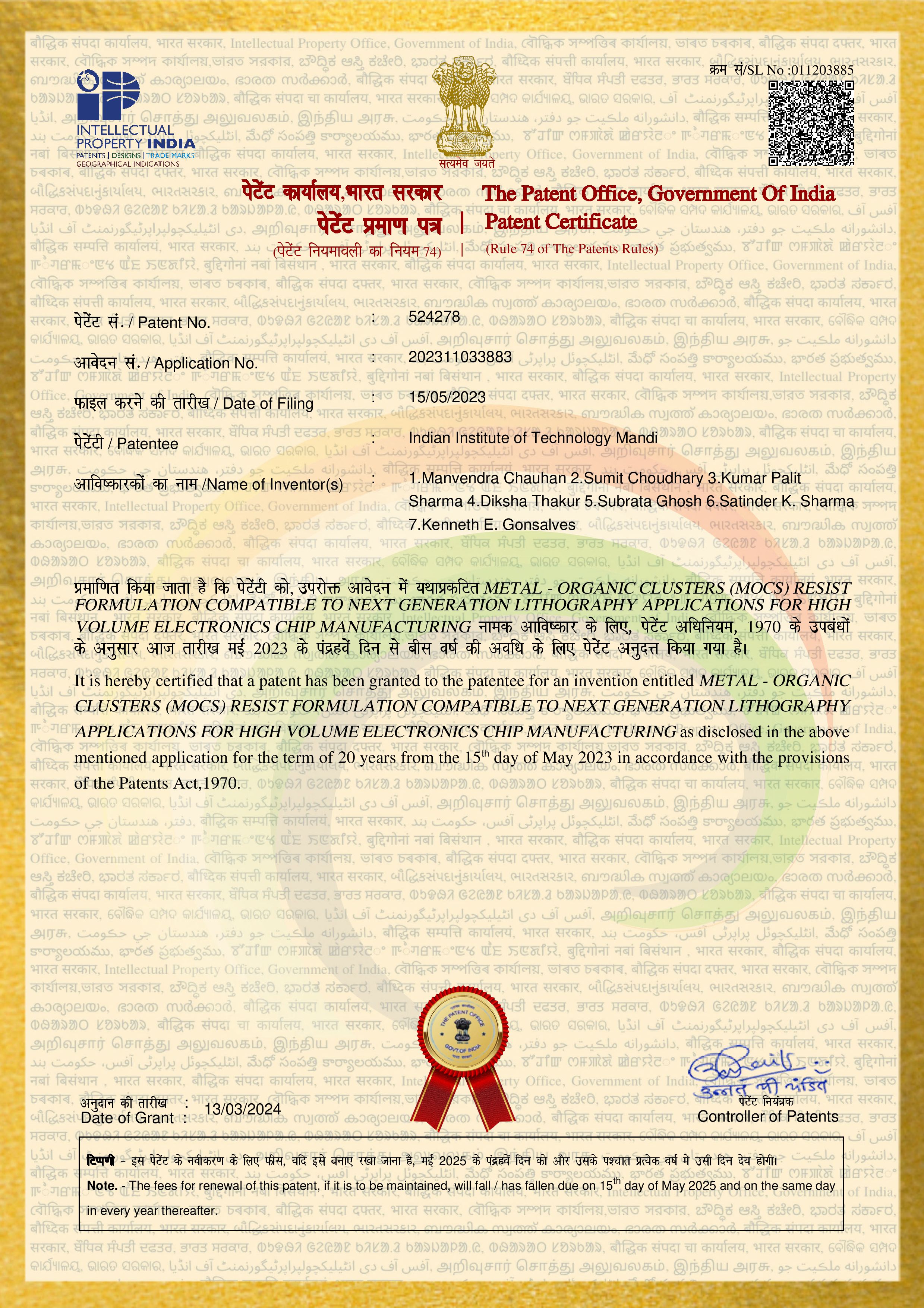
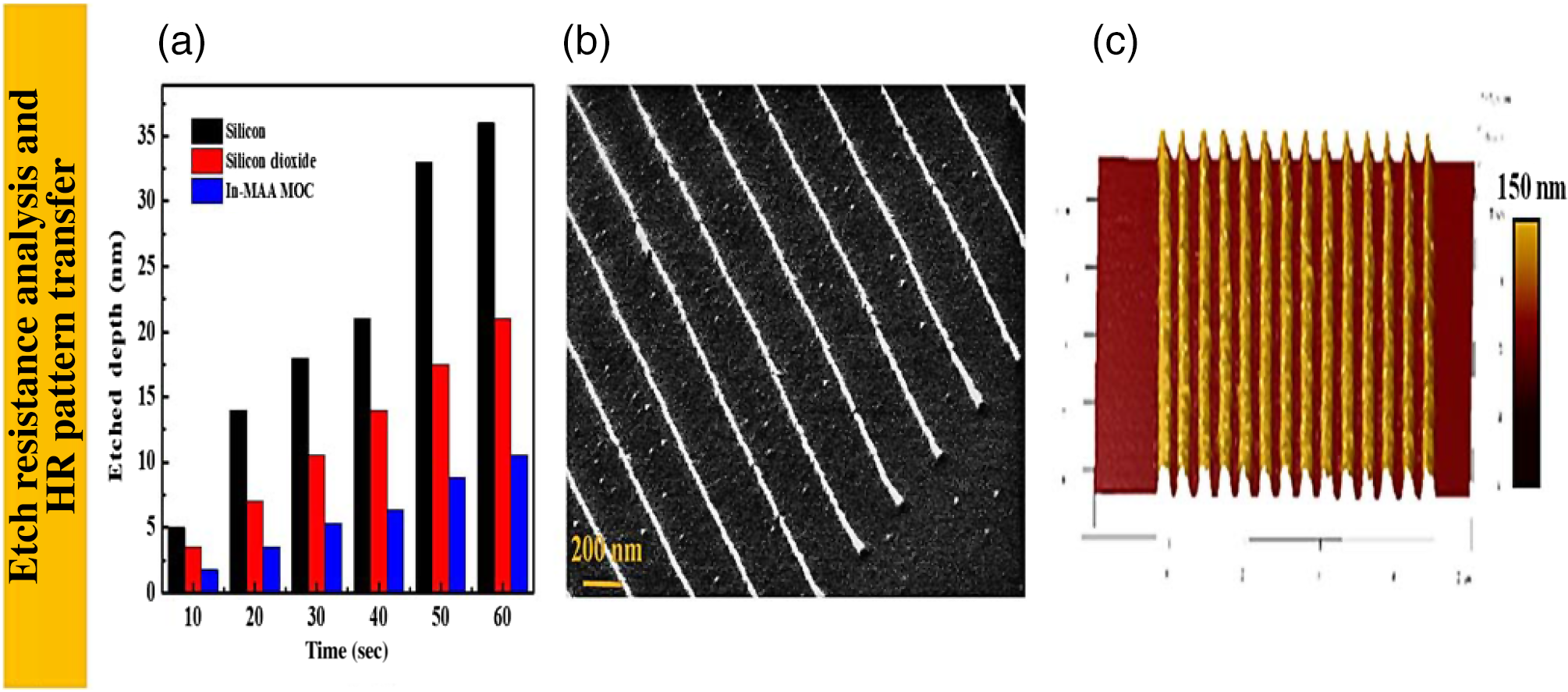
- Metal-Organic Clusters (MOCs) Resist Formulation Compatible to Next Generation Lithography Application.
Inventors: Manvendra Chauhan, Kumar Palit Sharma, Sumit Choudhary, Diksha Thakur, Subrata Ghosh,
Satinder K. Sharma, Kenneth E. Gonsalves. (Application number: 202311033883)
- Negative Tone Resist Compositions for Lithography
Inventors: Santu Nandi, Lalit Khilare, Mohamad G. Moinuddin, Sunil Kumar, Manvendra Chauhan,
Satinder K. Sharma, Subrata Ghosh, Kenneth E. Gonsalves. (Application number: 202111050981)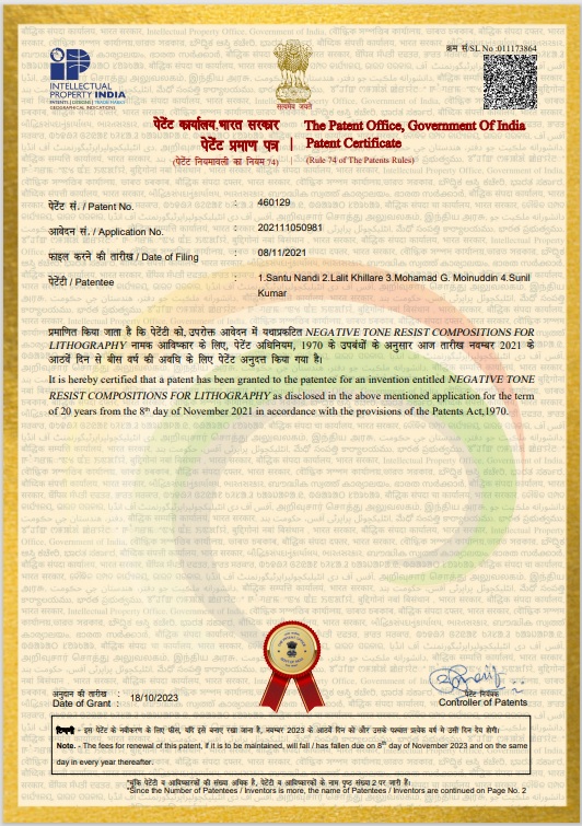
- A process for i-line resist dissolution dodulation using hydroxy-styrene based ter-polymer
Inventors: Santu Nandi, M.Yogesh, S.Dolai, Pradeep Parameswaran, Satinder K. Sharma, A. Bogavelly,
D.N.Tiwary, P. Jain, Subrata Ghosh, Kenneth Gonsalves. (Application number: 202141007495)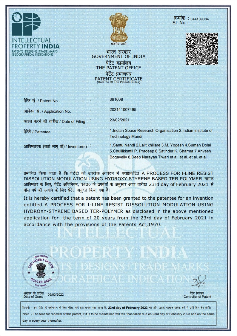
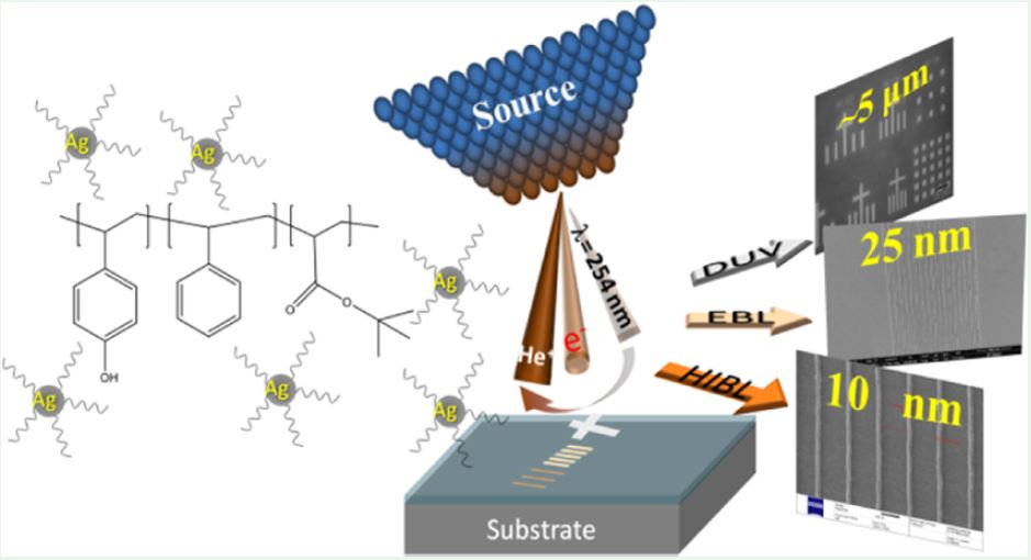
- Metal-organic Clusters (MOCs) Resist for Sub 10 nm Semiconductor Technology Node Patterning by
Helium Ion Beam (He + BL), and Electron Beam Lithography (EBL)
Inventors: Rudra Kumar, Manvendra Chauhan, M. G. Moinuddin, Satinder K. Sharma, Kenneth E. Gonsalves; (Application number: 202011003482)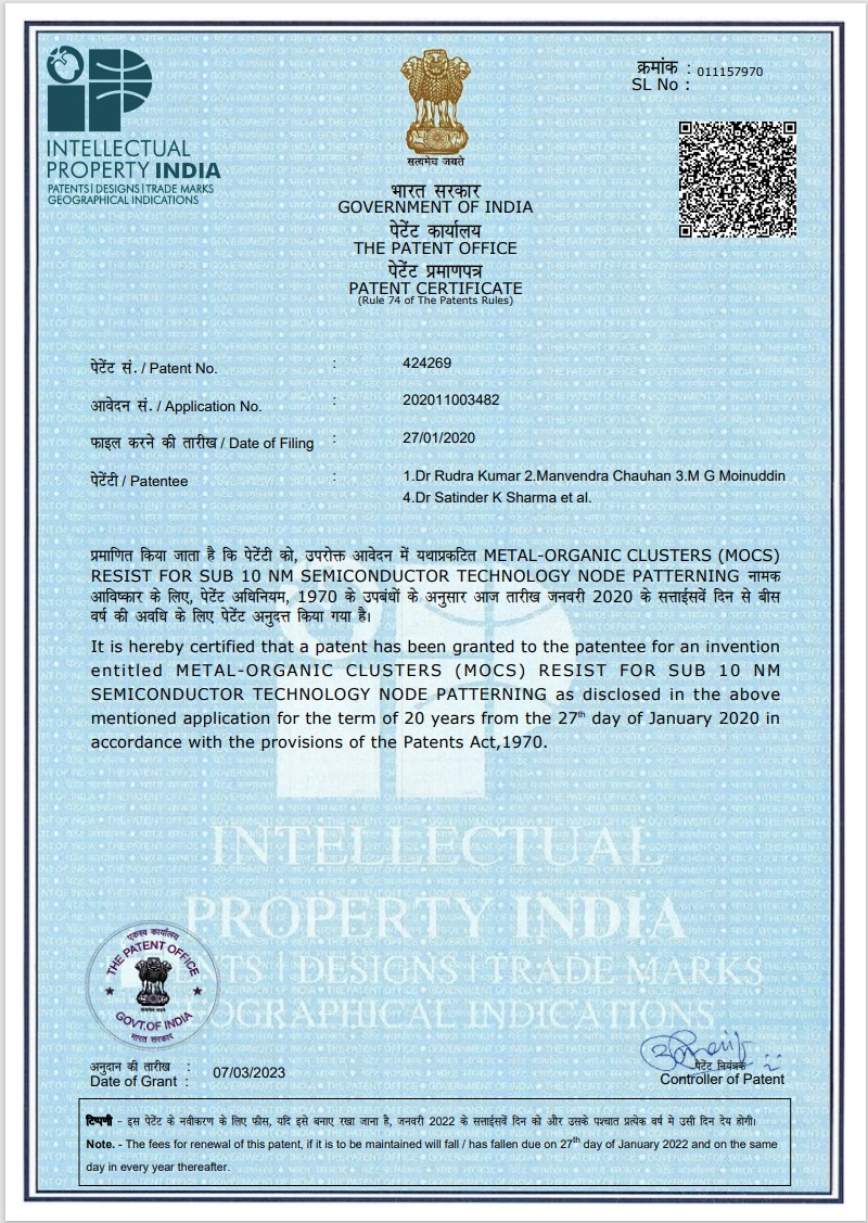
- A New Class of Non-Chemically Amplified Molecular Photoresists for Next Generation
Integrated Circuits (ICs) Technology
Inventors: Kenneth E Gonsalves; Subrata Ghosh; P. Parameswaran; Satinder K. Sharma; Neha Thakur;
Pulikanti Guru Prasad Reddy; Santu Nandi; M. Yogesh;(Application number: 201611044190)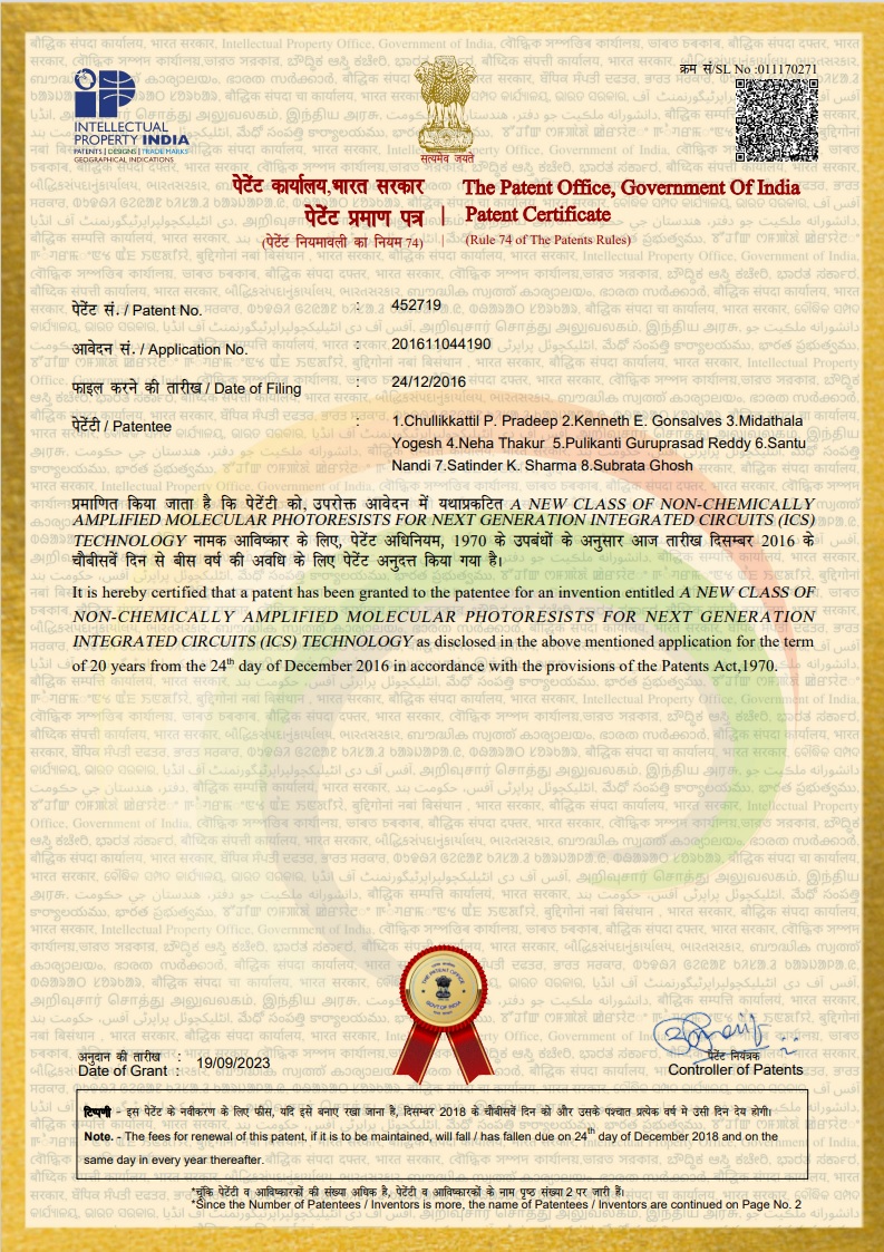
- Highly Sensitive MAPDSM-MAPDST based Resists Technology for Next Generation Lithography
Inventors: Kenneth E. Gonsalves, Satinder K. Sharma, Subrata Ghosh, Chullikkattil P. Pradeep,
Pulikanti Guruprasad Reddy, Satyendra P. Pal, Pawan Kumar. (Application number: 201611022219A).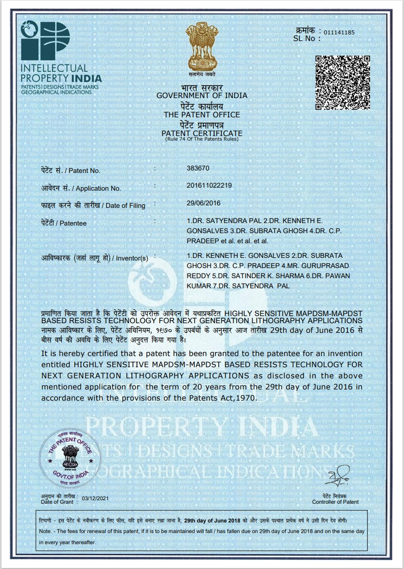
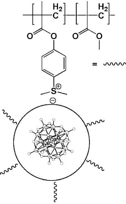
- Poly alkyl sulfide (PAS) synthesis, charecterization and its UV-365 nm lithography patterning
Inventors: Kenneth E. Gonsalves, Satinder K. Sharma, Subrata Ghosh, Chullikkattil P. Pradeep, Pulikanti Guruprasad Reddy, Satyendra P. Pal, Pawan Kumar. - Conceptual Hybrid Nano Photoresists for Sub-7 nm Node patterning Application.
Inventors: P.Guru Prasad Reddy, Kenneth E. Gonsalves, Subrata Ghosh, Satinder K. Sharma, Chullikkattil P. Pardeep (Application Number:- 201611028125). - Resist Technology Based on Polyarylene sulphide. (PAS) as a Unique Polymer Material for Semiconductor Fabrication Technology
Inventors: K. E. Gonsalves, S. Ghosh, C. P. Pradeep, P. G. Reddy, S. K. Sharma, S. P. Pal (Application number: IN 2016-11018061) - Non-Volatile Storage MRAM Technology Implying Alternate Tunnel Barrier
Inventors: Mohamad G. Moinuddin, Srikant Srivivasan, Satinder K. Sharma (Application number: 202211019370) - A One Step, Low Temperature, Cost Effective, Photo-Chemical Reduction of Graphene Oxide Dispersions for the Commercial Scale Analogous
reduced graphene oxide (r-GO) Production
Inventors: Satinder K. Sharma, M. Soni, P. Kumar, A.Soni. (Application Number:- 201611028125).
List of Published International Journals
-
(Kindly refresh page if this message is visible: "Requested article is not found in IHub.")
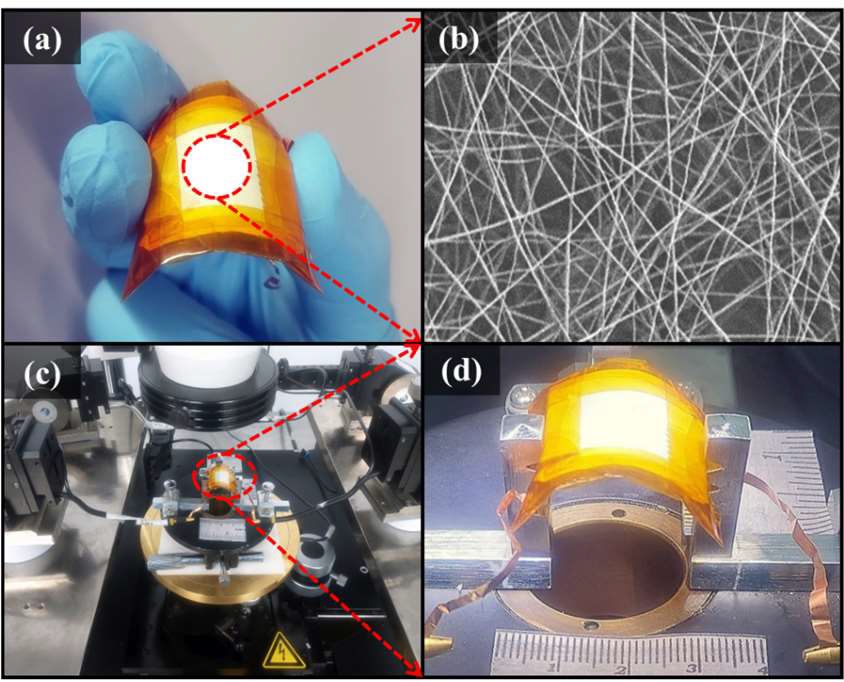
- Flexible ? - Phase PVDF-Cu-MAA Self-Powered Nanofiber Nanogenerator for Energy Harvesting Applications
Sachin, Sumit Choudhary, Satinder K. Sharma. IEEE Journal on Flexible Electronics (June, 2026) 10.1109/JFLEX.2026.3698890.

- N-Heterocycles for inducing high-sensitivity to inorganic resist compositions
Avik Das, Neha Thakur, Promit Chakraborty, Santu Nandi, Manvendra Chauhan, Gaurav Jayaswal, Dipanjan Dutta, Ambar Shukla, Nilesh Ladani, Prashant Varma, Santosh Kumar, Satinder K. Sharma, Subrata Ghosh. Proc. of SPIE Vol. 13983 139831U (2026) Doi: 10.1117/12.3090675.

- Dual-Component Functionalized Allylated Calix[4]arene-Dibutyltin Diacrylate Blends as Organic-Inorganic Hybrid Resist Compositions for Nanolithography
Promit Chakrabortya, Neha Thakur, Avik Das, Santu Nandi, Manvendra Chauhan, Prashant Varma, Nilesh Ladani, Ambar Shukla, Satinder K. Sharma, Subrata Ghosh. Proc. of SPIE Vol. 13983 139832B (2026) Doi: 10.1117/12.3090850.
 Link to the Poster
- Hybrid metal-organic clusters resist for next-generation high-NA EUV lithography
Neha, Manvendra Chauhan, Kumar Palit, Ashutosh Joshi, Ranbir Singh, Abhimanew Dhir, Robin Khosla, Bhaskar Mondal, Satinder K. Sharma, Ralph Dammel. Proc. of SPIE Vol. 13983 1398338 (2026) Doi: 10.1117/12.3091820.

- Systematic Investigation of Tin-Based Metal-Organic Cluster Resists for High-Resolution Next Generation Lithography
Sachin, Manvendra Chauhan, Neha, Meghana Sharma, Kumar Palit, Ashutosh Joshi, Satinder K. Sharma, Ralph Dammel. Proc. of SPIE Vol. 13983 1398339 (2026) Doi: 10.1117/12.3091826.

- Integrated Lith-To-Etch Protocols For Indigenous Resists Technology Enabling High-Fidelity Device Fabrication
Sumit Choudhary, Manvendra Chauhan, Satinder K. Sharma Proc. of SPIE Vol. 13984, 139840T (2026) Doi: 10.1117/12.3091257.

- Energy-Efficient Europium-Based 2D Perovskite ReRAM for Photo-Tunable Neuromorphic Computing
Manvendra Chauhan, Satinder K. Sharma IEEE Photonics Technology Letters (Page(s): 291 - 294, Volume: 38, Issue: 4, 15 February 2026) Doi: 10.1109/LPT.2025.3631106.

2025
- Electrospun P(VDF-TrFE):LiClO4 Hybrid Nanofiber-Based Highly Sensitive Piezocapacitive Pressure Sensors for Self-Powered Flexible Electronics
Pankaj kumar, Ranbir Singh, Satinder K. Sharma ACS Applied Electronic Materials, Vol. 13428, 1342809 (2025) Doi: 10.1021/acsaelm.5c00199.

- High-Performance Metal Organic Cluster Resists for High-NA Extreme Ultraviolet Lithography
Manvendra Chauhan1, Neha, Kumar Palit, Ranbir Singh, Abhimanew Dhir, Robin Khosla, Bhaskar Mondal, Satinder K. Sharma, Ralph Dammel, Ravi Kanjolia Advances in Patterning Materials and Processes XLII, Vol. 13428, 1342809 (2025) Doi: 10.1117/12.3052190.

2024
- Surface engineering of carbon fiber using microwave micro arcing (MwMA) for enhanced performance of resulting PEEK composites
Sudhir Kumar Chaudhary, Sunny Zafar, Satinder K. Sharma, Journal of Thermoplastic Composite Materials, Vol. 0(0) 1-20 (2024) DOI: 10.1177/08927057241298216.
- Low-Temperature Processed Ni/GeSn Optimal Contacts for Junctionless GeSn-on-Si FinFETs
Sumit Choudhary, Daniel Schwarz, Hannes S. Funk, Satinder K. Sharma, J�rg Schulze. IEEE Transactions on Electron Devices, Page(s): 5182 - 5189, Volume: 71, Issue: 9, September 2024) DOI: 10.1109/TED.2024.3430244.

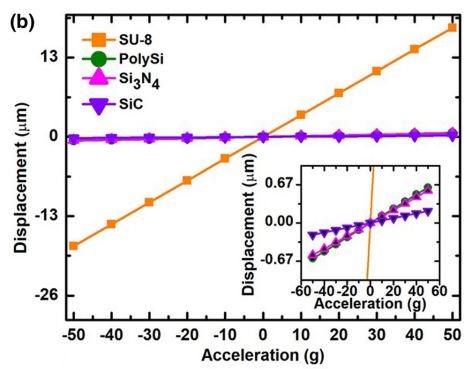
- Design and Simulation of Capacitive Z-axis MEMS Accelerometers using SU-8, PolySi, Si3N4, and SiC-based structural materials
Mandeep Jangra, Dhairya Singh Arya, Robin Khosla, Satinder K. Sharma 2020 5th IEEE International Conference on Emerging Electronics (ICEE)(2024) DOI: 10.1109/ICEE50728.2020.9776817

- Highly Sensitive Polymer Micro-Mesh for Measurement of Vacuum Packaged MEMS Devices
Manu Garg, Dhairya S. Arya, Mohamad G. Moinuddin, Satinder K. Sharma, Pushpapraj Singh 2020 5th IEEE International Conference on Emerging Electronics (ICEE)(2024) DOI: 10.1109/ICEE50728.2020.9776980

- Coupling of Triboelectric and Piezoelectric Effects in Nafion-Containing Polyvinylidene Fluoride: Lead Zirconium Titanate Nanofiber-Based Nanogenerators for Self-Powered Systems
Saira Bano, Bablesh Gupta, Satinder K. Sharma, and Ranbir Singh ACS Appl. Nano Mater. 7, 15425?15437 (2024) DOI: doi.org/10.1021/acsanm.4c02292

- Accepted: Pinch-Off Driven Near-ideal Output Characteristics of n-Ga2O3/p-GaN Light Effect Transistor for UV Photonics
Arnab Mondal, Manoj Kumar Yadav, Arpit Nandi1, Shiv Kumar Bishnoi, Indraneel Sanyal Satinder K. Sharma, Jen-Inn Chyi, and Ankush Bag Applied Physics Letters, Vol.125, Issue 2) (2024). DOI: 10.1063/5.0215146

- Accepted: Solution processed highly UVsensitive photodetector based on sub 5 nm Sn nanoparticles blended with TiO2 nanofiber
Shivani Sharma, Rishibrind Kumar Upadhyay, Nidhin S. Babu, Satinder K. Sharma. Journal of Alloys and Compounds (4 June, 2024). Doi.org/10.1016/j.jallcom.2024.175096 - Selective and Reversible Carbon Mono Oxide Gas Detection using Silver Doped Octahedral Molecular Sieves (OMS-2) Nanorods
Amit Kumar Gupta, Priyanshu Singh, Monical Jaiswal, Jagjiwan Mittal, Sivanandam Aravindan, Sumit Choudhary, Satinder K. Sharma, Robin Kumar. IOP Advances in Natural Sciences: Nanoscience and Nanotechnology (2024). - Sodium Niobate Nanowires Embedded PVA-Hydrogel-Based Triboelectric Nanogenerator for Versatile Energy Harvesting and Self-Powered CO Gas Sensor
Monical Jaiswal, Shivam Singh, Bharat Sharma, Sumit Choudhary, Robin Kumar, and Satinder K. Sharma. Nano Micro Small, (2024) DOI: 10.1002/smll.202403699

- Cost-Effective Processing of Flexible Tactile Sensors for e-skin Applications
Sachin, Sumit Choudhary, Ranbir Singh, Gopi Shrikanth Reddy, and Satinder K. Sharma. 8th IEEE Electron Devices Technology & Manufacturing Conference (EDTM), (2024) DOI: 10.1109/EDTM58488.2024.10512323

- Facile DUV Irradiated Solution-Processed ZrO2/In2O3 for Low Voltages FET Applications
Prachi Gupta, and Satinder K. Sharma. IEEE Transactions on Electron Devices, 1-9, (2024) DOI: DoI: 10.1109/TED.2024.3395422

- Electro-Optically Tunable Passivated Double-Cation Perovskite-Based ReRAM for Low-Power Memory Applications
Manvendra Chauhan, Ranbir Singh, Satinder K. Sharma. ACS Applied Electronic Materials (2024) DOI: doi.org/10.1021/acsaelm.4c00257

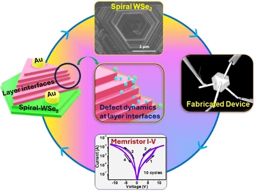
- Spiral WSe2 with Interlayer Twist for Memristive and Neuromorphic Device Applications
B. Raju Naik, Sumit Choudhary, Satinder K. Sharma, Vishwanath Balakrishnan. ACS Appl. Electron. Mater. (2024) DOI: doi.org/10.1021/acsaelm.3c01810

- Unveiling Thermal Effects on Sn-Doped -GaO Schottky Barrier Diodes on Sapphire for High-Temperature Power Electronics
Manoj K. Yadav, Arnab Mondal, Satinder K. Sharma, Ankush Bag. IEEE Transactions on Electron Devices,Volume 71, Issue 3, Page(s): 1529-1534 (2024) DOI: 10.1109/TED.2023.3333818
- Reliable Memristive Switching Empowered by Ag/NiO/W ReRAM Configuration for Multi-Level Non-Volatile Memory Applications
Manvendra Chauhan, Sumit Choudhary, Satinder K. Sharma. Advanced Electronic Materials, (2024) DOI: 10.1002/aelm.202300724
- Multifunctional fluorescent SPIONs display exceptional optical/magnetic contrast and enhanced photoconductivity in interdigitated electrode based photoresponsive devices
Ashish Tiwari, Ayan Debnath, Mohamad G. Moinuddin, Aamir Mushtaq, Anup Singh, Satinder K. Sharma Jaspreet K. Randhawa. Journal of materials Chemistry A, (2024) DOI: 10.1039/d3ta06147g
- Novel process integration flow of germanium-on-silicon FinFETs for low-power technologies
Sumit Choudhary, Midathala Yogesh, Daniel Schwarz, Hannes S. Funk, Subrata Ghosh, Satinder K. Sharma, J�rg Schulze, Kenneth E. Gonsalves. J. Vac. Sci. Technol. B 41, Volume 41, Issue 5 (2023) Doi: 10.1116/6.0002767
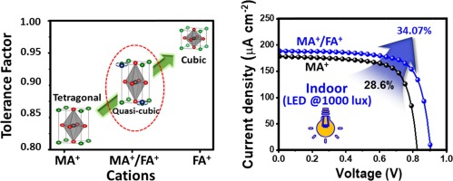
- Bandgap Engineered Double-Cation/Double-halide (DCDH) Quasi-Cubic Perovskite for Highly Efficient (> 36%) Indoor Photovoltaics
Ranbir Singh, Milon Kundar, Suman Kalyan Pal, Satinder K. Sharma. IEEE Journal of Photovoltaics,Vol:13, issue-6,858-865,(2023) DOI: 10.1109/JPHOTOV.2023.3300366
- Improvement of both performance and stability of photovoltaic devices by in situ formation of a sulfur-based 2D perovskite
Milon Kunder, Sahil Bhandari, Sein Chung, Kilwon Cho, Satinder K. Sharma, Ranbir Singh and Suman Kalyan Pal. Materials Science, 6, 4132-4140 (2023) Doi.org/10.48550/arXiv.2211.15236
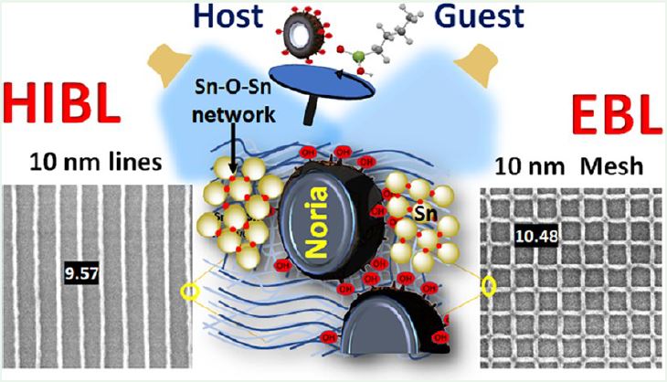
- Induced Chemical Networking of Organometallic Tin in a Cyclic Framework for Sub-10 nm Patterning and Interconnect Application
Santu Nandi, Lalit Khillare, Sunil Kumar, Mohamad G. Moinuddin, Manvendra Chauhan, Sumit Choudhary, Satinder K. Sharma, Subrata Ghosh and Kenneth E. Gonsalves. ACS Applied Nano Materials, 6, 4132-4140 (2023) doi.org/10.1021/acsanm.2c04831
- Rapid and reversible detection of trace amounts of H2S in air and packaged food using a biogenic bismuth oxide nanorod colorimetric sensor
Monica Jaiswal, Robin Kumar, Ravi Mani Tripathi, Ranu Nayak, Jagjiwan Mittal, Sumit Choudhary Satinder K. Sharma Sensors and Actuators: B. Chemical (2023). Doi.org/10.1016/j.snb.2023.133395
- Ultrasensitive metal-organic cluster resist for patterning of single exposure high numerical aperture extreme ultraviolet lithography applications
Manvendra Chauhan, Kumar Palit, Sumit Choudhary, Satinder K. Sharma and Kenneth E. Gonsalves Micro/Nanopatterning, Materials, and Metrology, Vol. 21, Issue 4, 044603 (December 2022). DOI: 10.1117/1.JMM.21.4.044603
- Hardware-Efficient and Short Sensing-Time Multicoset-Sampling Based Wideband Spectrum Sensor for Cognitive Radio Network
Rahul Sharma, Rahul Shrestha, Satinder K. Sharma. IEEE TRANSACTIONS ON CIRCUITS AND SYSTEMS-I (2022) Doi.org/10.1109/TCSI.2022.3223356
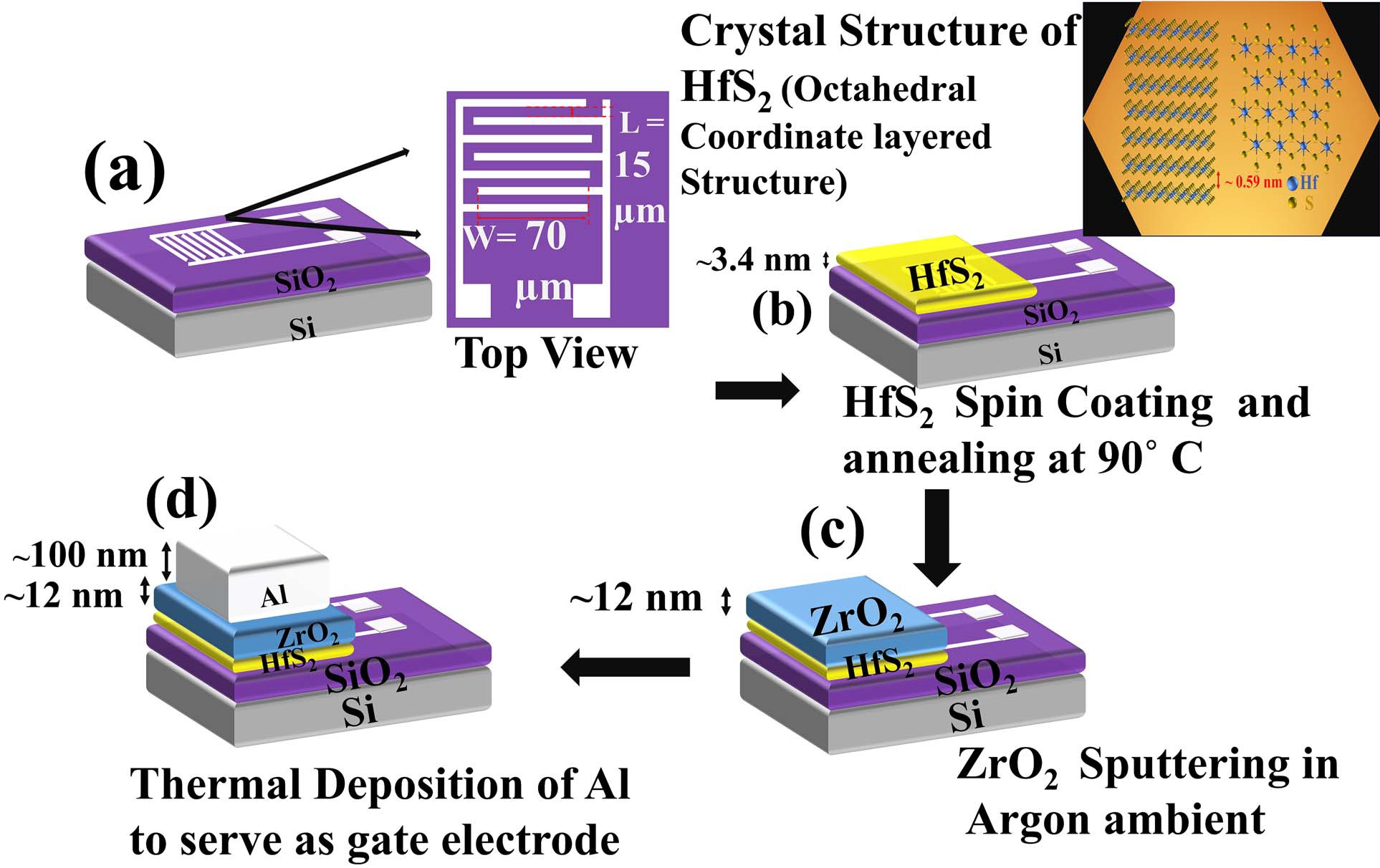
- Two-Dimensional Van Der Waals Hafnium Disulfide and Zirconium Oxide-Based Micro-Interdigitated Electrodes Transistors
Shivani Sharma, Subhashis Das, Robin Khosla, Hitesh Shrimali, Satinder K. Sharma. IEEE TRANSACTIONS ON ELECTRON DEVICES (2022,) Doi.org/10.1109/TED.2022.3202510
- Highly efficient quasi-cubic structured perovskite for harvesting energy from artificial indoor LED light source
Ranbir Singh, Vivek Kumar Shukla, Mritunjaya Parashar, Vikrant Sharma, Satinder K. Sharma. Solar Energy, Volume 245, Pages 332-339 (2022,) Doi.10.1109/JFLEX.2022.3189946
- Light-sensitive PVDF-TrFE:PDI Hybrid Nanofibersbased Flexible Bimodal Piezoelectric Nanogenerator
Pankaj Kumar, Sumit Choudhary, Kumar Palit Sharma, Satinder K. Sharma, Ranbir Singh. IEEE Journal on Flexible Electronics (2022) Doi.org/10.1016/j.solener.2022.09.015
- Macrocycle Network-Aided Nanopatterning of Inorganic Resists on Silicon
Santu Nandi, Lalit Khillare, Mohamad G. Moinuddin, Sunil Kumar, Manvendra Chauhan, Satinder K. Sharma, Subrata Ghosh, Kenneth E. Gonsalves. Applied Nano Materials, 5, 8, 10268�10279 (2022) Doi.org/10.1021/acsanm.2c01321
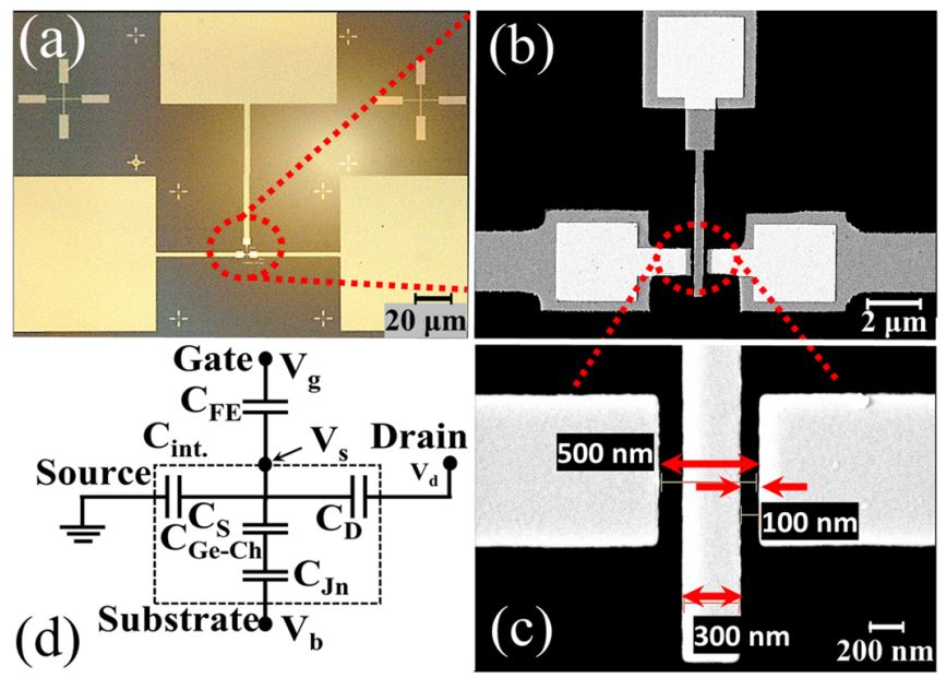
- A Steep Slope MBE-Grown Thin p-Ge Channel FETs on Bulk GeSi Using HZO Internal Voltage Amplification
Sumit Choudhary, Daniel Schwarz, Hannes S. Funk, D. Weibhaupt, Robin Khosla, Satinder K. Sharma, Jorg Schulze IEEE Transactions on Electron Devices, VOL. 69, NO. 5, (2022) 10.1109/TED.2022.3161857
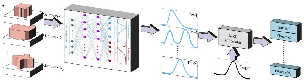
- Deep Learning approach for inverse design of metasurfaces with a wider shape gamut
Soumyashree S. Panda, Sumit Choudhary, Siddharth Joshi, Satinder K. Sharma, Ravi S. Hegde. Optics Letter Vol. 47, No. 10, (2022) Doi.org/10.1364/OL.458746
- Organotin bearing polymeric resists for electron beam lithography
Midathala Yogesh, Mohamad G. Moinuddin, Lalit D. Khillare, Srinivas Chinthalapalli, Satinder K. Sharma, Subrata Ghosh, and Kenneth E. Gonsalves. Microelectronic Engineering Volume 260, (2022) 111795 doi.org/10.1016/j.mee.2022.111795
- Low-Latency and Reconfigurable VLSI-Architectures for Computing Eigenvalues and Eigenvectors Using CORDIC-Based Parallel Jacobi Method
Rahul Sharma, Rahul Shrestha, Satinder K. Sharma IEEE Transactions on Very Large Scale Integration Systems, (2022) doi.org/10.1109/TVLSI.2022.3170526
- Integration of Ferroelectric Materials: An Ultimate Solution for Next-Generation Computing and Storage Devices
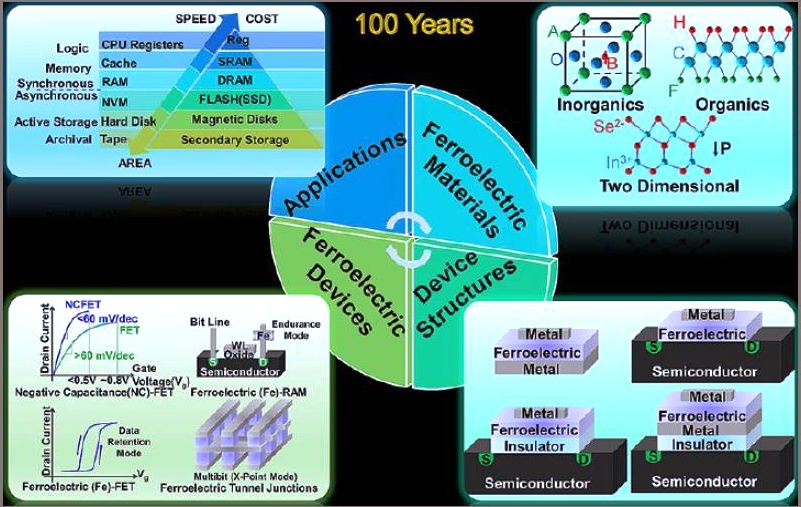
Robin Khosla,Satinder K. Sharma ACS Appl. Electron. Mater. 2021, 3, 2862-2897, doi.org/10.1021/acsaelm.0c00851
- Probing Ferrimagnetic Semiconductor with Enhanced Negative Magnetoresistance: 2D Chromium Sulfide
Mohamad G. Moinuddin, Srikant Srinivasan, Satinder K. Sharma Advanced Electronic Materials, Volume7, Issue9 (2021), Doi.org/10.1002/aelm.202001116
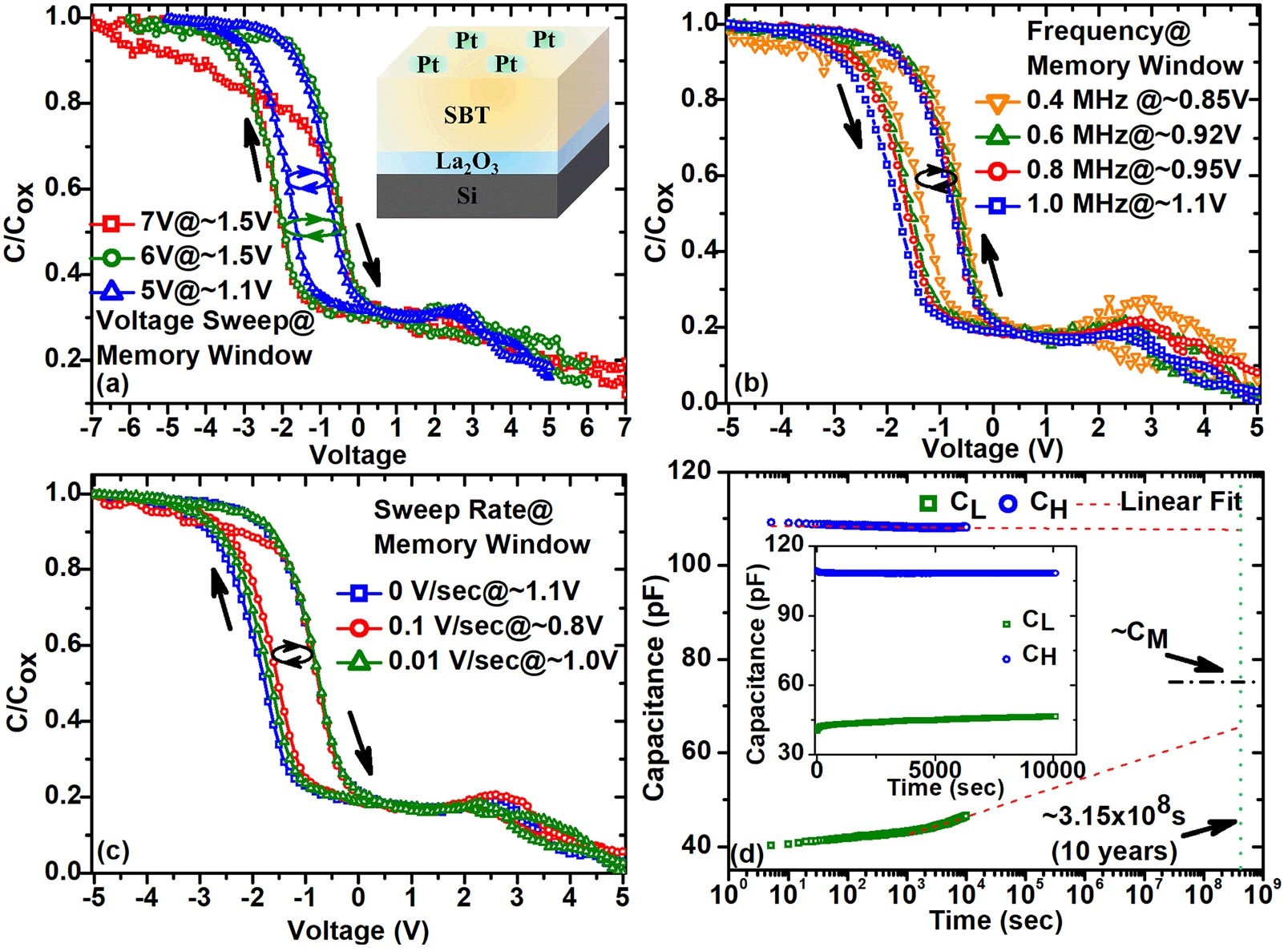
- Metal (Pt)/ferroelectric (SrBi2Ta2O9)/insulator (La2O3)/semiconductor (Si), MFIS structures for nonvolatile memory applications
Shivendra K. Rathaur, Robin Khosla, Satinder K. Sharma Applied Physics Letter (2021), doi.org/10.1063/5.0055792
- Nanoscale Probing of Surface Charges in Functional Copper-Metal Organic Clusters by Kelvin Probe Force Microscopy for Field-Effect Transistors
Rudra Kumar, Prachi Gupta, Satinder K. Sharma Advance Materials Interfaces 2021, doi.org/10.1002/admi.202100529
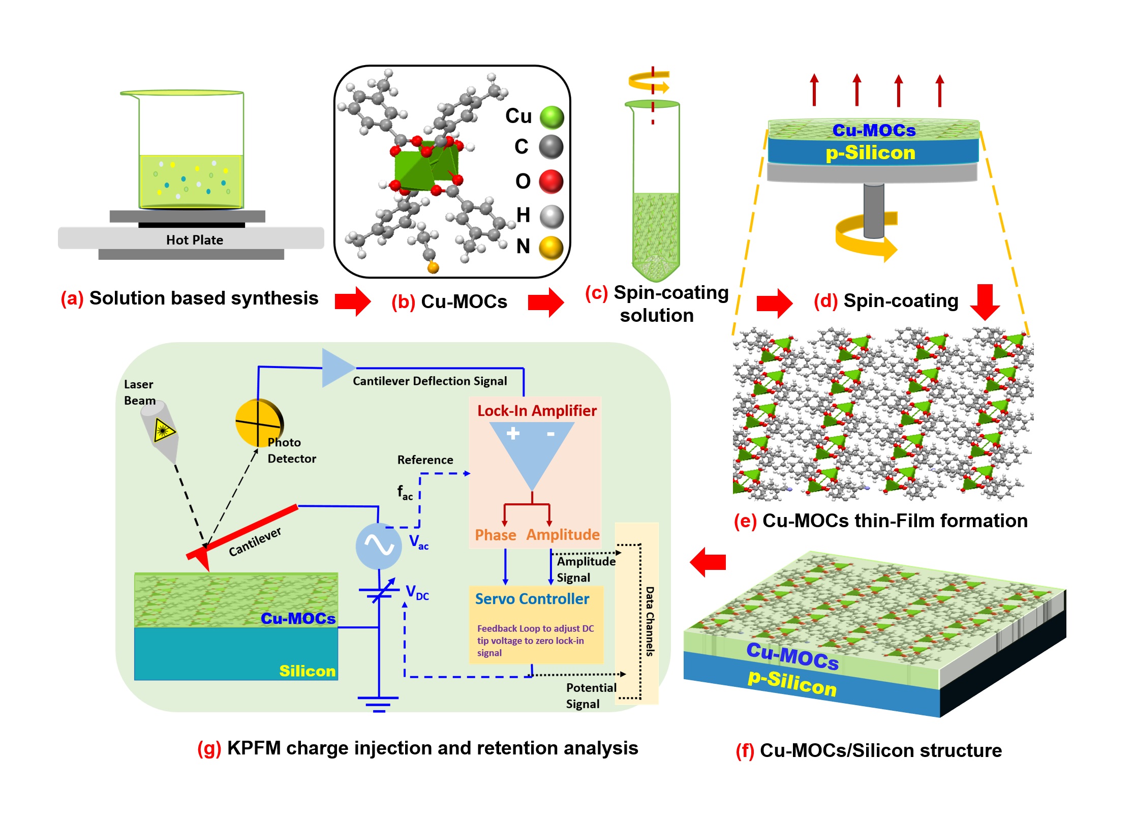
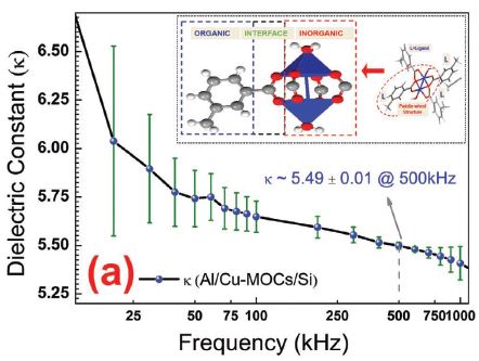
- Integration of High-Performance Cost-Effective Copper-Metal-Organic-Nanocluster-based Gate Dielectric for Next-Generation CMOS Applications
Prachi Gupta, Rudra Kumar, Satinder K. Sharma Adv. Electron. Mater. 2021, Doi 10.1002/aelm.202000835
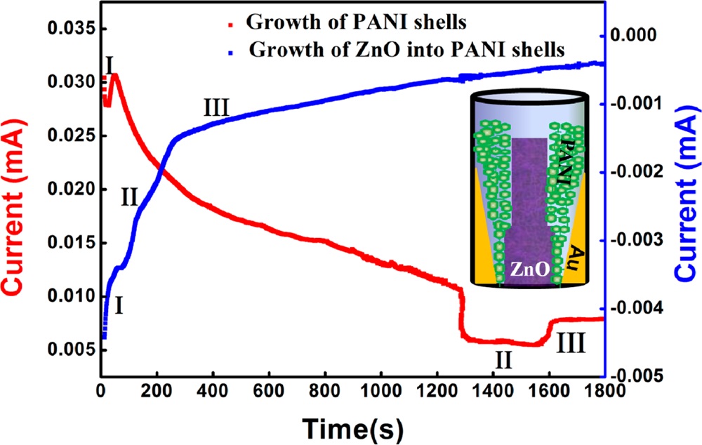
- An efficient hydrogen gas sensor based on hierarchical Ag/ZnO hollow microstructures
Sonalika Agarwal, Sanjay kumar, Himanshu Agrawal, Mohamad G. Moinuddin, Manoj Kumar, Satinder K. Sharma, Kamlendra Awasthi. Sensors and Actuators: B. Chemical (2021), Doi.org/10.1016/j.snb.2021.13051
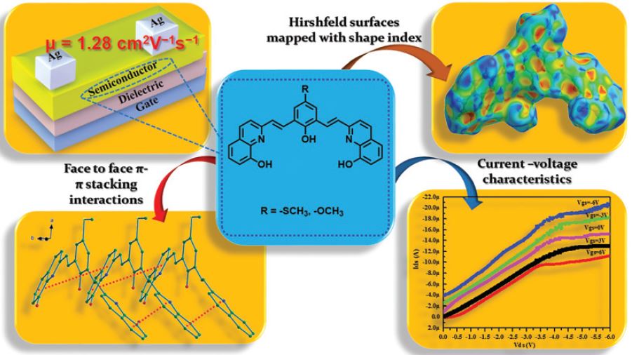
- 2,2'-(Arylenedivinylene)bis-8-hydroxyquinolines exhibiting aromatic p-p stacking interactions as solution-processable p-type organic semiconductors for high-performance organic field effect transistors
Suman Sehlangia, Shivani Sharma,Satinder K. Sharma, Chullikkattil, P. Pradeep Materials Advances, 2021, 00,1-10 (2021), 10.1039/d1ma00215e
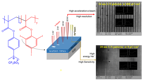
- Organoiodine Functionality Bearing Resists for Electron-Beam and Helium Ion Beam Lithography: Complex and Sub-16 nm Patterning
Midathala Yogesh,Mohamad. G. Moinuddin, Manvendra Chauhan,Satinder K. Sharma, Subrata Ghosh, Kenneth E. Gonsalves ACS Applied Electronic Materials (2021), doi.org/10.1021/acsaelm.0c01120
- Maskless lithography: an approach to SU-8 based sensitive and high-g Z-axis polymer MEMS accelerometer
Mandeep Jangra, Dhairya Singh Arya, Robin Khosla,Satinder K. Sharma. Microsystem Technologies (2021) doi.org/10.1007/s00542-021-05217-0(0123456789)
- Substrate Orientation Dependent Current Transport Mechanisms in �-Ga2O3/Si based Schottky Barrier Diodes
Manoj K Yadav, Arnab Mondal, Ankush Bag, Satinder K. Sharma. Journal of Vacuum Science & Technology A 39, 033203 (2021) doi:10.1116/6.0000858
- Development of Metal-Organic Cluster based Negative Tone Resist: Pre-screened through the Helium-ion Beam prelude to Extreme Ultraviolet Lithography (EUVL) Applications
Satinder K. Sharma, Manvendra Chauhan, Rudra Kumar, Kumar Palit, Sumit Choudhary, and Kenneth E. Gonsalves. Advances in Patterning Materials and Processes XXXVIII Vol. 11612, 1161208 (2021) doi: 10.1117/12.2583850
 Link to the Presentation
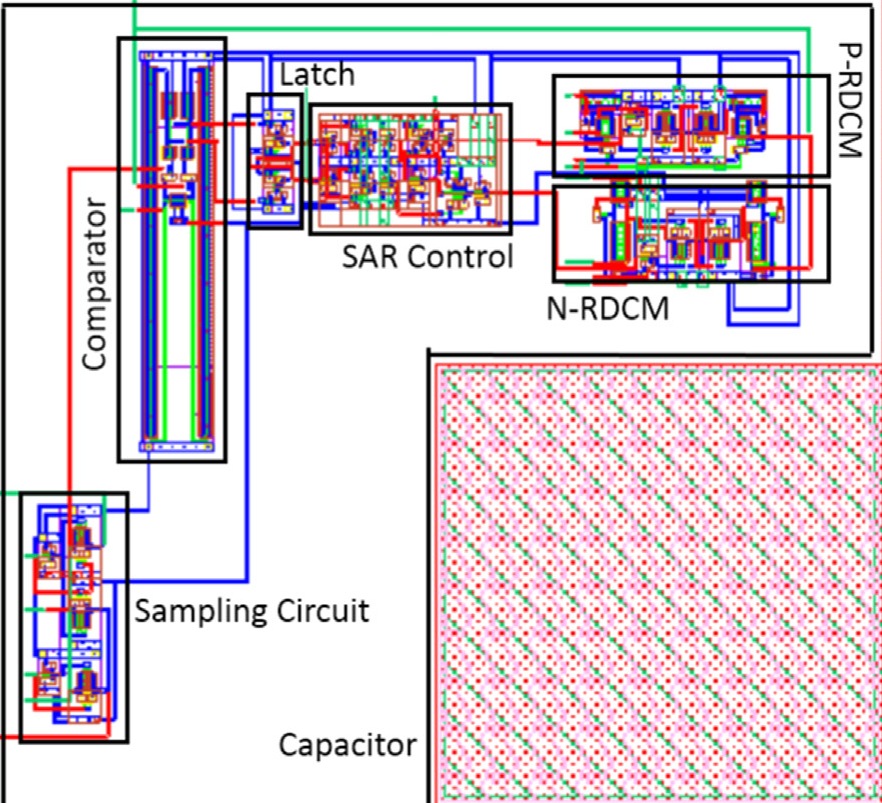
- Digitally Assisted Secondary Switch-and-Compare Technique for a SAR ADC
Ashish Joshi, Hitesh Shrimali, Satinder K. Sharma. IEEE Transactions on Circuits and Systems II, Volume:68, Issue;7 Pages 1549-7747, I.P <2.5 (2021), 10.1109/TCSII.2021.3053210
- Integration of high-performance cost-effective copper-metal-organic-nanoclusters based gate dielectric for next-generation CMOS applications
Prachi Gupta, Rudra Kumar, Satinder K. Sharma. Advanced Electronic Materials (2021) DOI:10.1002/aelm.202000835
- Resists for Helium Ion Beam Lithography: Recent Advances
Nagarjuna Ravi Kiran, Manvendra Chauhan, Subrata Ghosh, Satinder K. Sharma and Kenneth E. Gonsalves. ACS Applied Electronic Materials (2020);
- A Discrete-Time MOS Parametric Amplifier-Based Chopped Signal Demodulator
Ashish Joshi, Hitesh Shrimali, Satinder K. Sharma; , IEEE Transactions on Very Large Scale Integration (VLSI) System (2020); 10.1049/iet-cds.2019.0224

- NrGO Floating Gate and Ultra thin SiOxNy Tunneling layer based Al/PMMA/ NrGO/SiOXNY/p-Si/Au gate stack for Reliability Analysis of Flash Memory
Mahesh Soni, Ajay Soni, and Satinder K. Sharma; IEEE Transactions on Device and Materials Reliability (2020); 10.1109/TDMR.2020.3010267
- Functionalized Ag Nanoparticles Embedded in Polymer Resists for High-Resolution Lithography
Mohamad G. Moinuddin, Rudra Kumar, Midathala Yogesh, Shivani Sharma, Manoj Sahani, Satinder K. Sharma and Kenneth E. Gonsalves. ACS Applied Nano Materials (2020); 10.1109/TDMR.2020.3010267
- Reduced switching mode for an SAR ADC: analysis and design of an SAR A-to-D algorithm with periodic stand-by mode circuit components
Ashish Joshi, Hitesh Shrimali, Satinder K. Sharma; IET Circuits, Devices & Systems, (2020); 10.1049/iet-cds.2019.0224
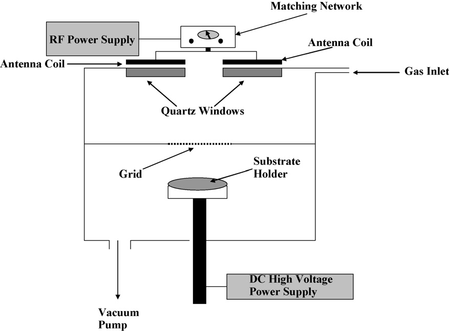
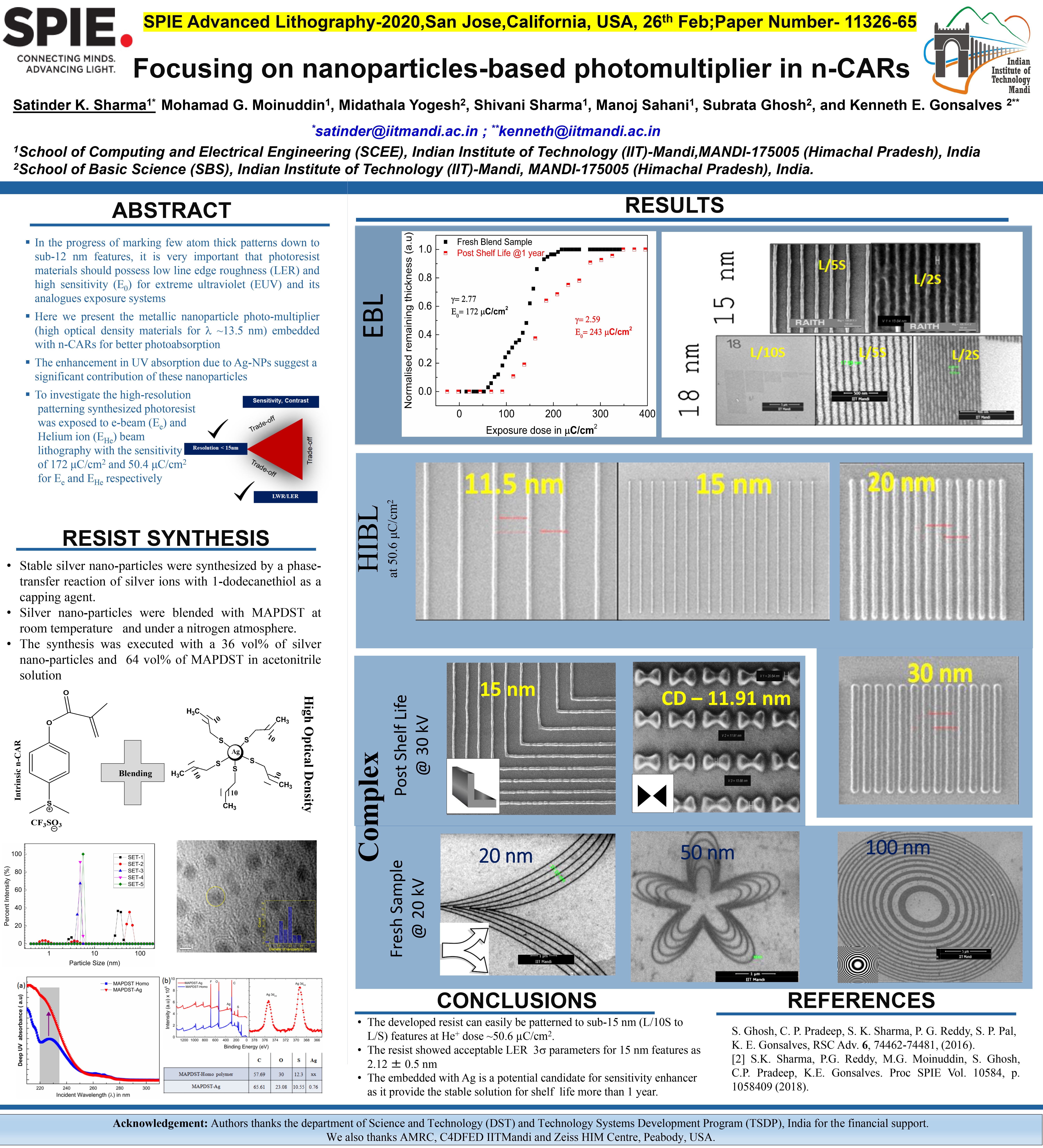
- Focusing on nanoparticles based photomultiplier in n-CARs
Satinder K. Sharma, Mohamad G. Moinuddin, Midathala Yogesh, Shivani Sharma, Manoj Sahani, Subrata Ghosh, and Kenneth E. Gonsalves; Proceedings Volume 11326, Advances in Patterning Materials and Processes XXXVII; 113261C, (2020); 10.1117/12.2552190
- All new nickel based Metal Core Organic Cluster (MCOC) resist for N7+ node patterning
Satinder K. Sharma, Rudra Kumar, Manvendra Chauhan, Mohamad G. Moinuddin, Jerome Peter, Subrata Ghosh, Chullikkattil P. Pradeep, and Kenneth E. Gonsalves; Proceedings Volume 11326, Advances in Patterning Materials and Processes XXXVII; 1132604, (2020); 10.1117/12.2552189
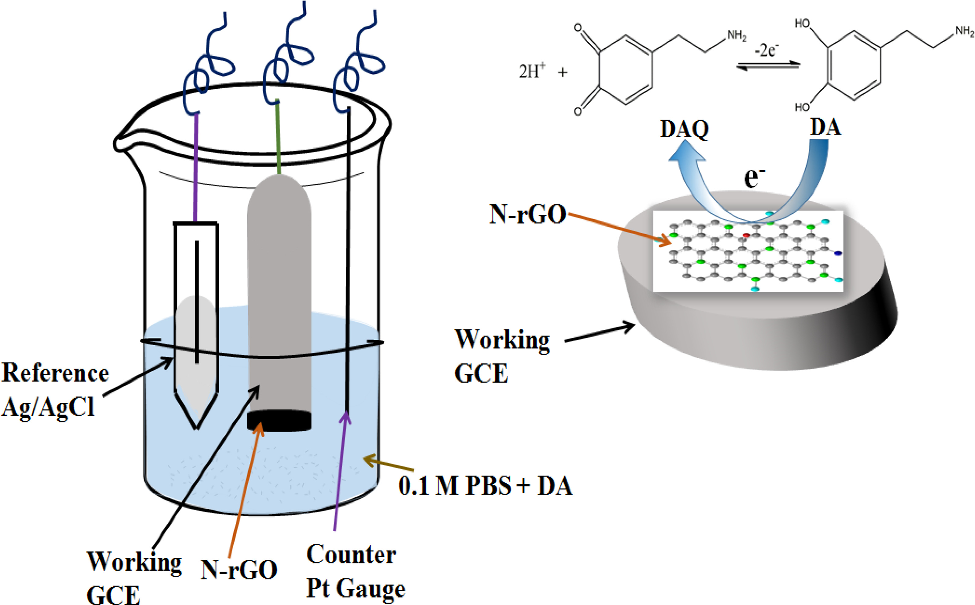
- Highly sensitive electrochemical sensing of neurotransmitter dopamine from scalable UV irradiation-based nitrogen-doped reduced
graphene oxide-modified electrode
Richa Soni, Kumar Palit, Mahesh Soni, Rudra Kumar and Satinder K. Sharma; Bulletin of Materials Science, (2020); 10.1007/s12034-020-02091-w
- Mechanistic Insights of Sn-Based Non-Chemically-Amplified Resists under EUV Irradiation
Guilherme K. Belmonte, Suelen W. Cendron, Pulikanti Guruprasad Reddy, Cleverson A.S. Moura, Mohamad Ghulam Moinuddin, Jerome Peter, Satinder K. Sharma, Gabriela Lando, Marcelo Puiatti, Kenneth E. Gonsalves, Daniel E.Weibel; Applied Surface Science, (2020); 10.1016/j.apsusc.2020.146553
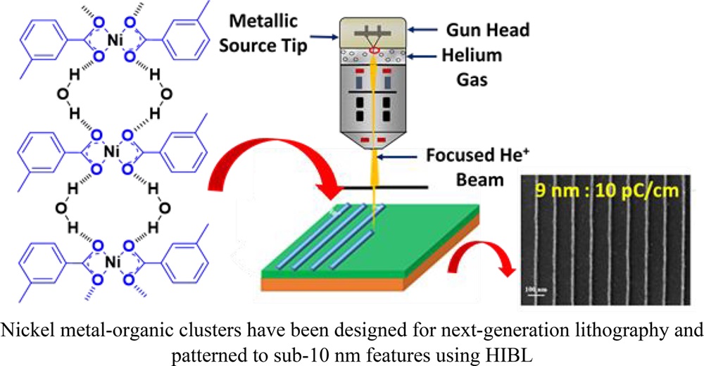
- Development of Nickel-Based Negative Tone Metal Oxide Cluster Resists for Sub-10 nm Electron Beam and Helium Ion Beam Lithography
Rudra Kumar, Manvendra Chauhan, Mohamad G. Moinuddin, Satinder K. Sharma, and Kenneth E. Gonsalves; ACS Applied Materials & Interfaces, (2020); 10.1021/acsami.9b21414
- Organotin in Nonchemically Amplified Polymeric Hybrid Resist Imparts Better Resolution with Sensitivity for Next-Generation Lithography
Jerome Peter, Mohamad G. Moinuddin, Subrata Ghosh, Satinder K. Sharma, and Kenneth E. Gonsalves; ACS Applied Polymer Materials, (2020); 10.1021/acsapm.0c00005
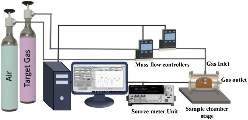
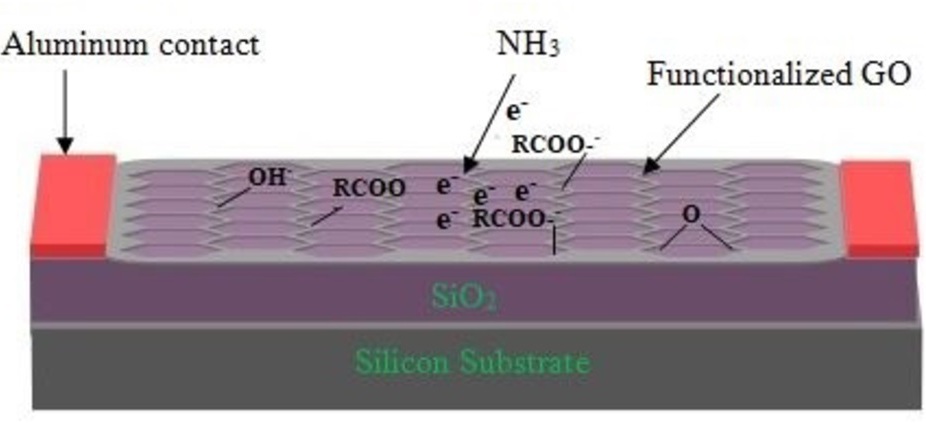
- Room temperature ammonia gas sensor using Meta Toluic acid functionalized graphene oxide
Ravi Kumar, Anil Kumar, Rakesh Singh, Rajesh kashyap, Rajiv Kumar, Dinesh Kumar, Satinder K. Sharma, Mukesh Kumar, Materials Chemistry and Physics 240, 121922, (2019); 10.1016/j.matchemphys.2019.121922
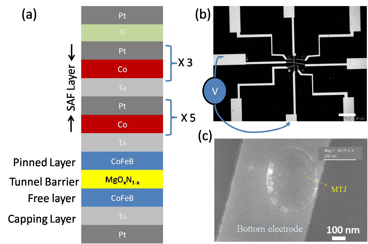
- Low-Current-Density Magnetic Tunnel Junctions for STT-RAM Application Using MgO x N1-x (x = 0.57) Tunnel Barrier
M. G. Moinuddin, Aijaz. H. Lone, Shivangi Shringi, Srikant Srinivasan and Satinder K Sharma, IEEE Transactions on Electron Devices, (2019); 10.1109/TED.2019.2954131
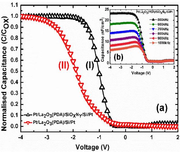
- Alternate lanthanum oxide/silicon oxynitride-based gate stack performance enhancement due to
ultrathin oxynitride interfacial layer for CMOS applications
Prachi Gupta, Mahesh Soni, Satinder K. Sharma; Journal of Materials Science: Materials in Electronics,vol 31, pp-1986-1995, Dec (2019); 10.1007/s10854-019-02718-7
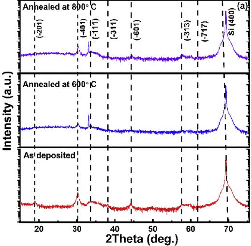
- Impact of annealing temperature on band-alignment of PLD grown Ga2O3/Si (100) heterointerface
Manoj K. Yadav, Arnab Mondal, Subhashis Das, Satinder K. Sharma, Ankush Bag, Journal of Alloys and Compounds; 153052, 16 November (2019); 10.1016/j.jallcom.2019.153052
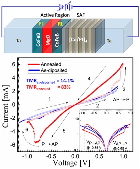
- Realization of large area Co20Fe60B20 based p-magnetic tunnel junction for CMOS compatible device application
Mohamad G. Moinuddin, Aijaz Lone, Srikant Srinivasan, and Satinder K. Sharma, ACS Applied Electronic Materials, (2019); 10.1021/acsaelm.9b00469
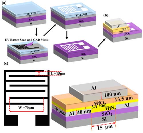
- Realization and Performance Analysis of Facile Processed �-IDE based multi-layer HfS2/HfO2 Transistors
Shivani Sharma, Subhashis Das, Robin Khosla, Hitesh Shrimali, Satinder K. Sharma; IEEE Transaction on Electron Devices, Volume: 66, Issue: 7, July (2019); 10.1109/TED.2019.2917323
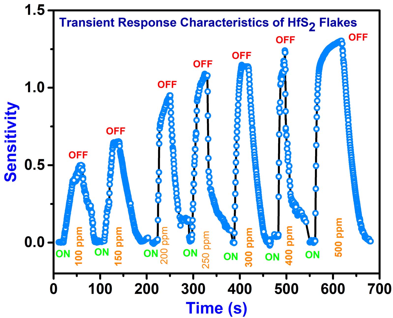
- Facile Synthesis of 2D-HfS2 Flakes/�-IDE based Highly Sensitive and Selective Sensor for Methanol
Sensing Application at Room Temperature
Subhashis Das, Shivani Sharma and Satinder K. Sharma; IEEE Sensors Journal, 26 June (2019); 10.1109/JSEN.2019.2925027
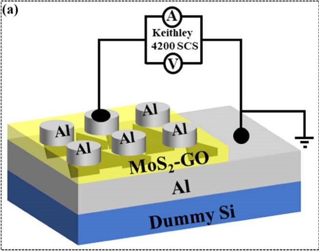
- Low Voltage & Controlled Switching of MoS2-GO Resistive Layers based ReRAM for Non-Volatile Memory Applications
Sumit Choudhary, Mahesh Soni, and Satinder K. Sharma; Semicond. Sci. Technol.34, 085009, 11pp, (2019); 10.1088/1361-6641/ab2c09
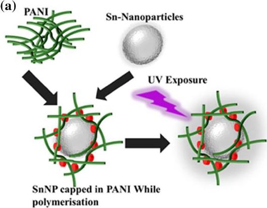
- Highly UV sensitive Sn Nanoparticles blended with polyaniline onto Micro-Interdigitated Electrode Array for UV-C detection applications
Shivani Sharma, Subhashis Das, Robin Khosla, Hitesh Shrimali, and Satinder K. Sharma; Journal of Materials Science: Materials in Electronics; Vol. 30, Issue 8, pp 7534-7542, (2019); 10.1007/s10854-019-01067-9
- Ferrocene Bearing Non-ionic Poly-aryl Tosylates: Synthesis, Characterization and Electron Beam Lithography Applications
Pulikanti Guruprasad Reddy, M.G.Moinuddin, Aneesh M.Joseph, Santu Nandi, Midathala Yogesh, Subrata Ghosh, Chullikkattil P. Pradeep , Satinder K. Sharma, Kenneth E. Gonsalves; Journal of Photopolymer Science and Technology, Volume 31, Number 6, pp-669-678, (2018); 10.2494/photopolymer.31.669
- Evaluation of high-resolution and sensitivity of n-CAR hybrid resist for sub-16nm or below technology node
Satinder K. Sharma, Mohamad Ghulam Moinuddin, Pulikanti Guruprasad Reddy, Chullikkattil P. Pradeep, Subrata Ghosh, and Kenneth E. Gonsalves; Proc. SPIE 10583, Extreme Ultraviolet (EUV) Lithography IX, 105831Q, SPIE Advanced Lithography, (2018); 10.1117/12.2297565
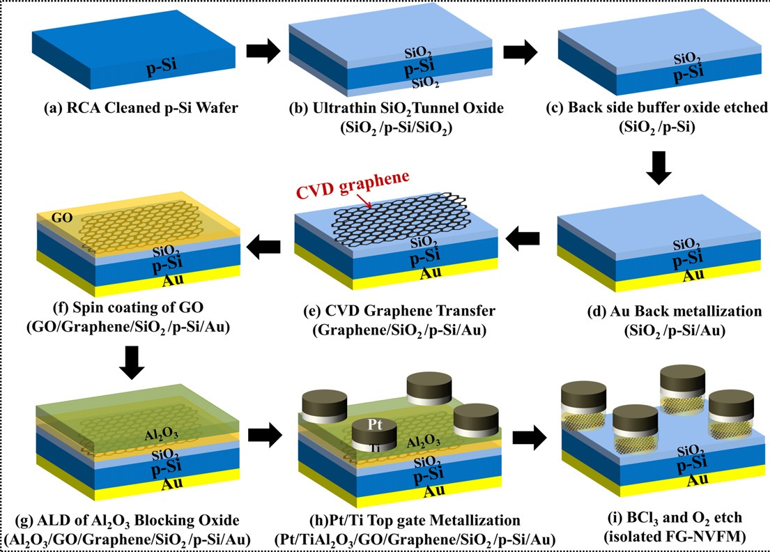
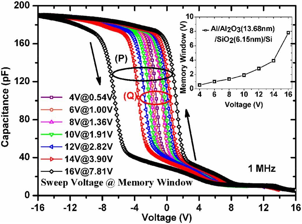
- Integration of graphene oxide buffer layer/graphene floating gate for wide memory window in
Pt/Ti/Al2O3/GO/graphene/SiO2/p-Si/Au non-volatile (FLASH) applications
Mahesh Soni, Ajay Soni, and Satinder K. Sharma, Applied Physics Letters, 112, 252102, (2018); 10.1063/1.5030020
- Helium ion active hybrid non-chemically amplified resist (n-CAR) for sub-10 nm patterning applications
Satinder K. Sharma, Pulikanti Guruprasad Reddy, Mohamad Ghulam Moinuddin, Subrata Ghosh, Chullikkattil P. Pradeep, and Kenneth E. Gonsalves; Proc. SPIE 10584, Emerging Patterning Technologies, 1058409, SPIE Advanced Lithography, (2018); 10.1117/12.2297537
- High-Performance CSA-PANI based Organic Phototransistor by Elastomer Gratings
Shivani Sharma, Robin Khosla, Subhashis Das, Hitesh Shrimali, and Satinder K. Sharma; Journal of Organic Electronics, vol 57; pp-14-20, (2018); 10.1016/j.orgel.2018.02.031
- Investigations on structural, optical and magnetic properties of Fe and Dy co-doped ZnO nanoparticles
Jaskaran Singh; Arun Kumar Singh; Robin Khosla; Satinder K. Sharma; Gyaneshwar Sharma; Sanjeev Kumar; Journal of Materials Science: Materials in Electronics, vol 29, pp-850-385, (2018); 10.1007/s10854-017-8321-4
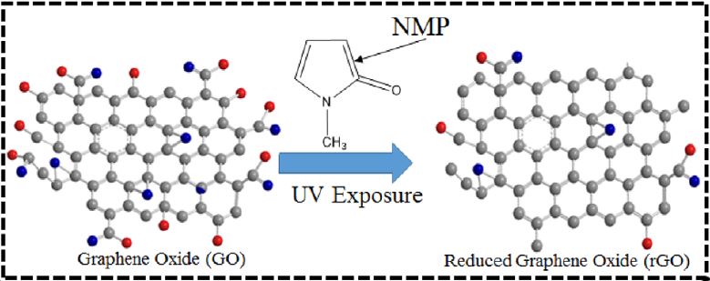
- Scalable and site specific functionalization of reduced graphene oxide for circuit elements and flexible electronics
Mahesh Soni, Pawan Kumar, Juhi Pandey, Satinder K. Sharma, Ajay Soni; Carbon; Vol. 128, Pages 172-178, (2018); 10.1016/j.carbon.2017.11.087
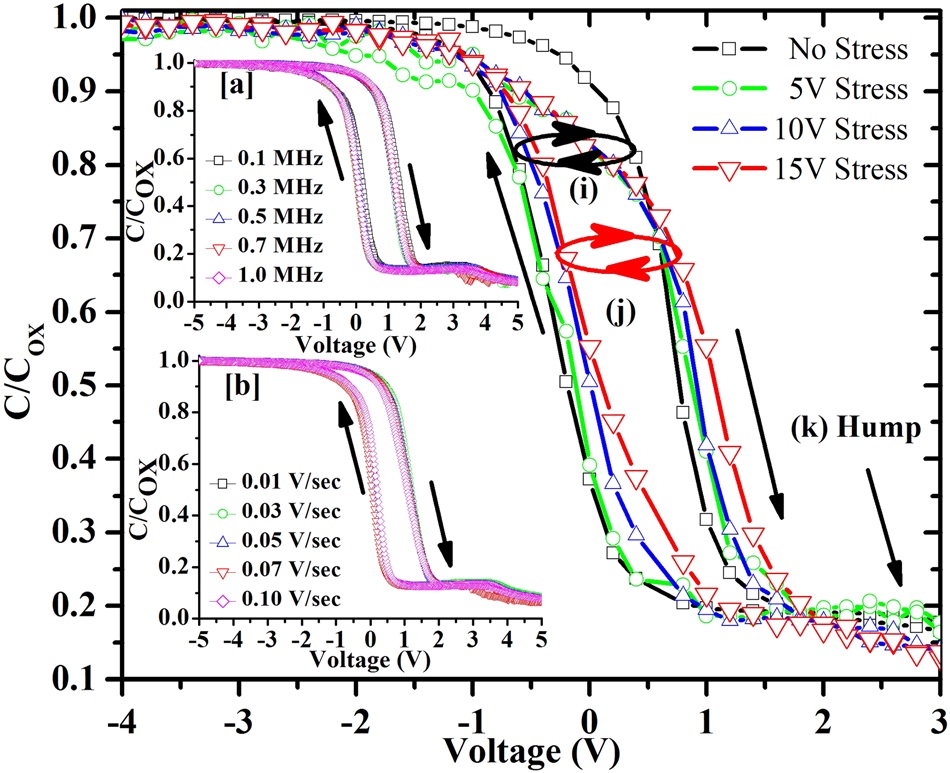
- Frequency Dispersion and Efficient Capacitance Correction Method in High-? MOS Capacitors based on C-V and C-F Measurements
Robin Khosla and Satinder K. Sharma; Journal of Vacuum Science & Technology-B (JVST-B); vol 36, 012201, (2018); 10.1116/1.4995809
- Enhanced nano-mechanical properties of the high resolution EUVL patterns of MAPDSA-MAPDST resists containing
hexafluoro antimonate
Pawan Kumar, Pulikanti Guru Prasad Reddy, Satinder K. Sharma, Subrata Ghosh, Chullikkattil P. Pradeep and Kenneth E. Gonsalves; Journal of Microelectronics Engineering, (2018); 10.1016/j.mee.2018.03.014
- Design of a Charge Sensitive Amplifier for Particle Detection Application in BCD 180 nm Technology
H.Shrimali, A.Joshi, E. Ruscino, I. Yadav, Satinder K. Sharma, V. Liberali, and A. Andreazza; Journal of Instrumentation; JINST_018P_0917; September 7, (2017).
- New non-chemically amplified molecular resist design with switchable sensitivity for multi-lithography
applications and nanopatterning
Neha Thakur; Pulikanti Reddy, Santu Nandi, Yogesh, Midathala; Satinder K. Sharma, Chullikkattil Pradeep, Subrata Ghosh, Kenneth Gonsalves, Journal of Micromechanics and Microengineering, IOP Science, (2017); 10.1088/1361-6439/aa8751
- Organic-Inorganic Hybrid Photoresists Containing Hexafluoroantimonate: Design, Synthesis and High Resolution EUV
Lithography Studies
Pulikanti Guruprasad Reddy, Pawan Kumar, Subrata Ghosh, Chullikkattil P. Pradeep, Satinder K. Sharma, and Kenneth E. Gonsalves; Materials Chemistry Frontiers, (2017); 10.1039/c7qm00343a
- Nitrogen Doped Multilayer Photo Catalytically Reduced Graphene Oxide Floating Gate:
Al/PMMA/NrGO/SiO2/p-Si/Au based Hybrid Gate Stack for Non Volatile Memory Applications
Mahesh Soni, Ajay Soni, Satinder K. Sharma; Journal of Organic Electronics, vol 51, (2017); 10.1016/j.orgel.2017.09.011
- Photoacid generator integrated terpolymer for electron beam lithography applications:
sensitive resist with pattern transfer potential
Santu Nandi, Midathala Yogesh, P. Guru Prasad Reddy, Satinder K. Sharma, Chullikkattil P. Pradeep, Subrata Ghosh and Kenneth E Gonsalves; Mater.Chem.Front., vol 1, pp-1895-1899, (2017); 10.1039/C7QM00140A
- Highly-Sensitive Surface-Enhanced Raman Scattering (SERS) based Multi Gas Sensor:
Au nanoparticles decorated on partially embedded 2D colloidal crystals into elastome
Satinder K. Sharma, Pawan Kumar, Sumit Barthwal, Seema Sharma and Ashutosh Sharma, Chemistry Select, vol 2, pp-6961-6969, (2017); 10.1002/slct.201701204
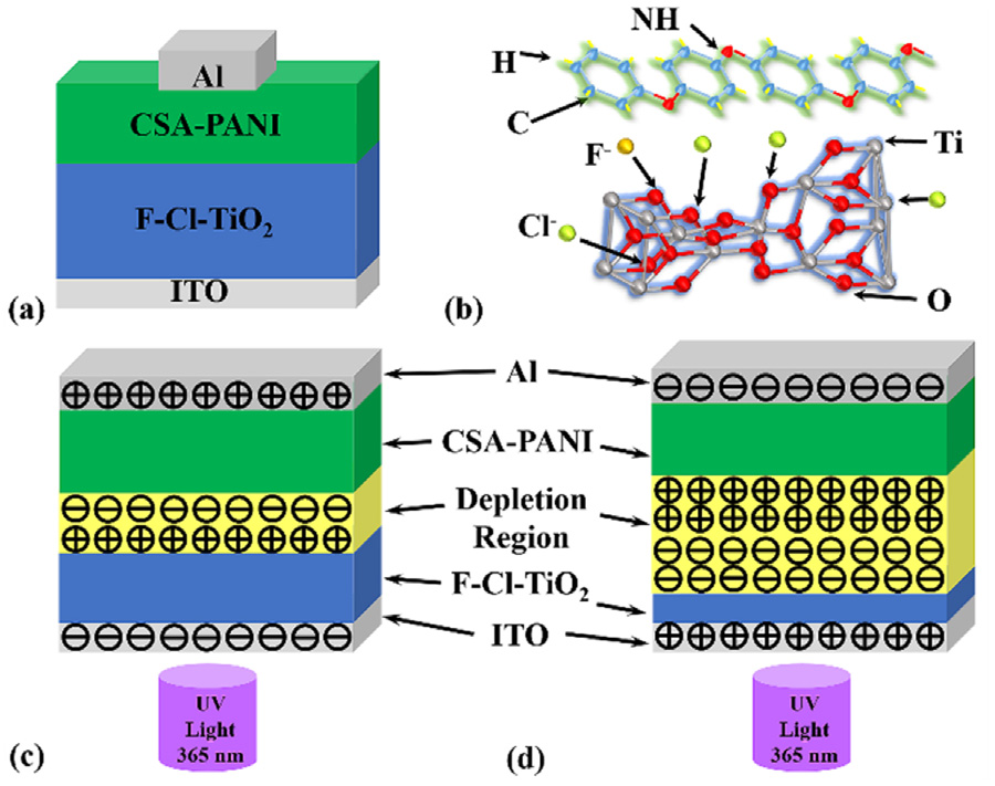
- Fluorine-Chlorine co-doped TiO2/CSA doped Polyaniline based high performance
inorganic/organic hybrid heterostructure for UV photodetection applications
Shivani Sharma, Robin Khosla, Dinesh Deva, Hitesh Shrimali and Satinder K. Sharma; Sensors and Actuators A Physical, 261, April (2017); 10.1016/j.sna.2017.04.043
- Photo-Catalytic Reduction of Oxygenated Graphene Dispersions for Supercapacitor Applications
Mahesh Soni, Pawan Kumar, Rudra Kumar, Satinder K. Sharma and Ajay Soni; Journal of Physics. D: Appl. Phys.,vol 50, 124003, 8pp, (2017); 10.1088/1361-6463/aa5c9f
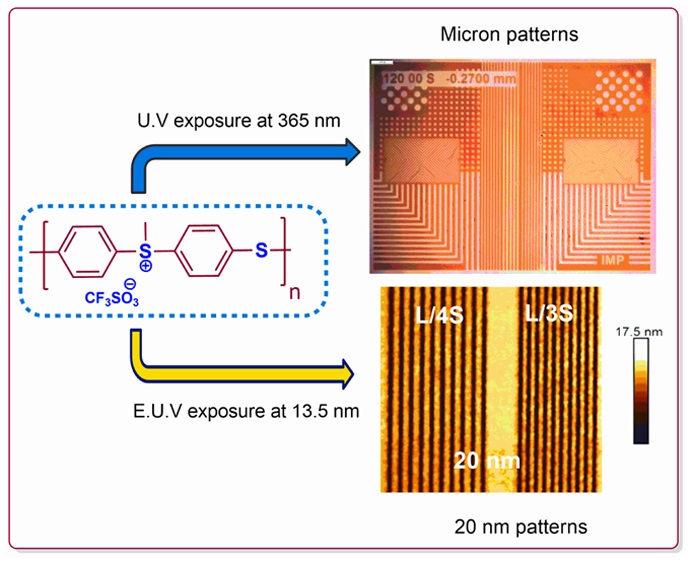
- Polyarylenesulfonium salt as a novel and versatile non-chemically amplified negative tone photoresist for
high resolution EUV lithography applications
Pulikanti Guruprasad Reddy, Satyendra Prakash Pal, Pawan Kumar, Chullikkattil P. Pradeep, Subrata Ghosh, Satinder K. Sharma, Kenneth E. Gonsalves; ACS Appl. Mater. Interfaces, vol 9 (1), pp 17-21, (2017); 10.1021/acsami.6b10384
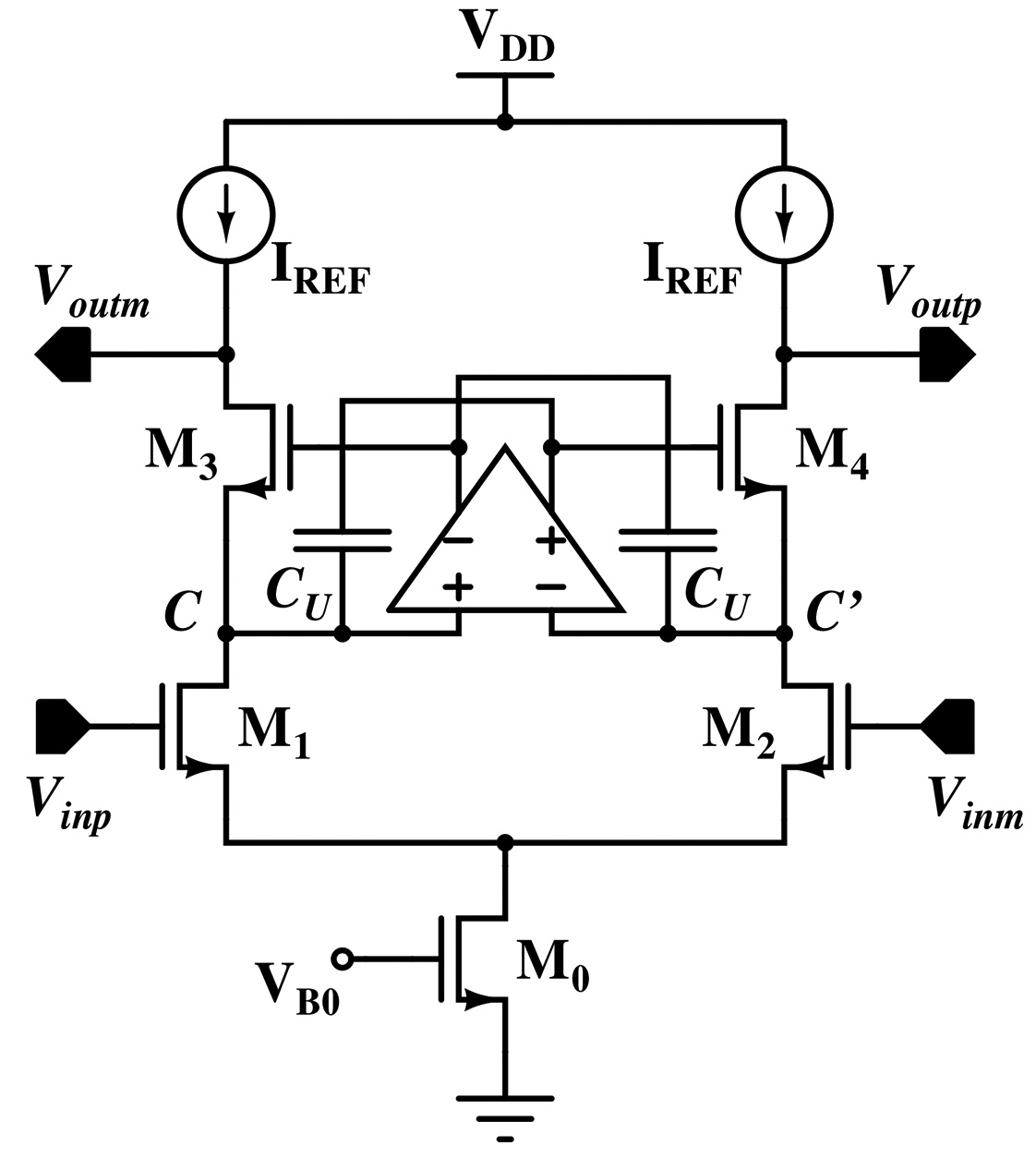
- A Systematic Design Approach for a Gain Boosted Telescopic OTA with Cross Coupled Capacitor
Ashish Joshi, Hitesh Shrimali and Satinder K. Sharma; IET Circuits, Devices & Systems, Vol. 11 Iss. 3, pp. 225-231, (2017). 10.1049/iet-cds.2016.0448
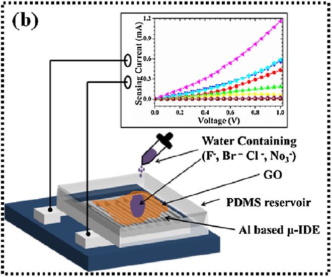
- Selective detection of F- using Al microarrays integrated graphene oxide
M. Soni, P. Kumar, A. Soni, Satinder K. Sharma; Sensors and Actuators B: Chemical, Volume 247, Pages 224-227, (2017); 10.1016/j.snb.2017.02.142
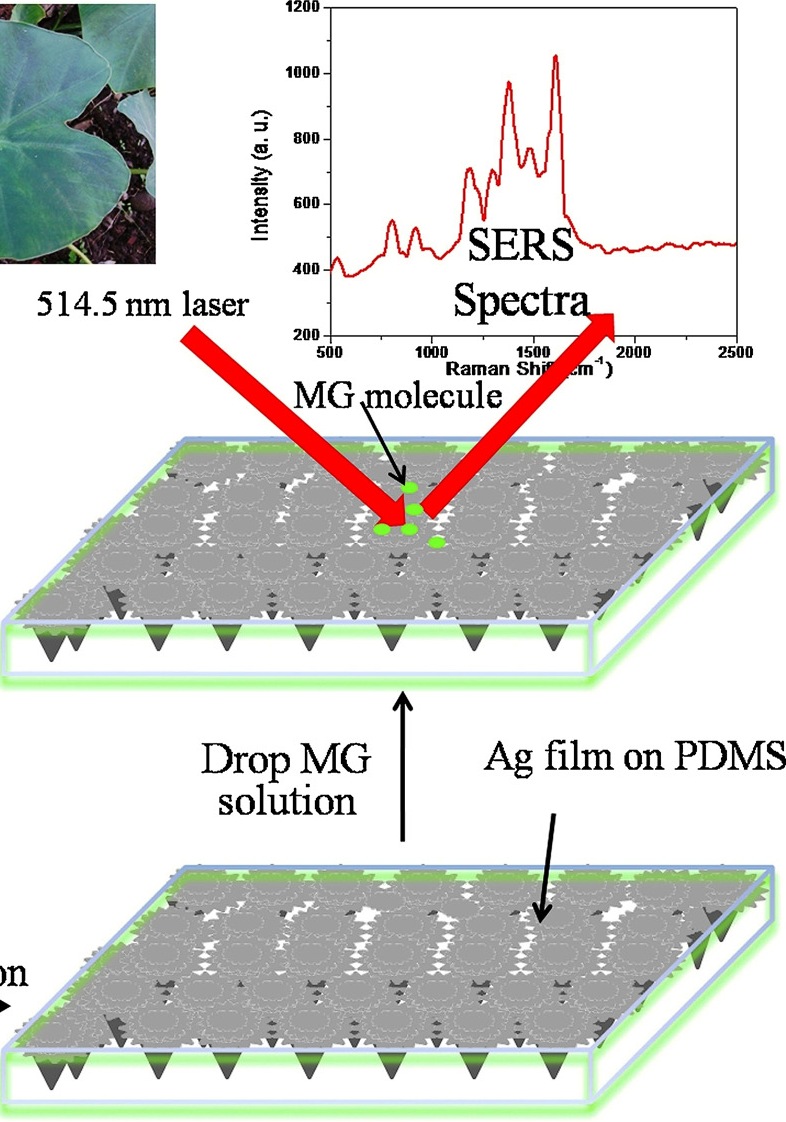
- A highly sensitive, flexible SERS sensor for malachite green detection based on Ag decorated microstructured
PDMS substrate fabricated from Taro leaf as template
Pawan Kumar, Robin Khosla, Mahesh Soni, Dinesh Deva and Satinder K. Sharma; Sensor and Actuators B: Chemical, Volume 246, Pages 477-486, (2017); 10.1016/j.snb.2017.01.202
- Charge Trapping Analysis of Metal/Al2O3/SiO2/Si, gate stack for emerging embedded memories
Robin Khosla, Erlend Rolseth, Pawan Kumar, Senthil Srinivasan V Palayam, Satinder K. Sharma and Jorg Schulze; IEEE Transactions on Device and Materials Reliability, Volume: 17, Issue: 1, March (2017); 10.1109/TDMR.2017.2659760
- Design and Development of Low Activation Energy based Non Chemically Amplified (n-CARs) Resists for Next
Generation EUV Lithography
Satinder K. Sharma, Satyendra Prakash Pal, Pulikanti Guruprasad Reddy, Pawan Kumar, Subrata Ghosh and Kenneth E. Gonsalves, Microelectronic Engineering, vol 164, pp-115-122, (2016); 10.1016/j.mee.2016.07.017
- Recent advances in non-chemically amplified photoresists for next generation IC technology
Subrata Ghosh, Chullikkattil P. Pradeep, Satinder K. Sharma, Pulikanti Guruprasad Reddy, Satyendra P. Pal and Kenneth E. Gonsalves; RSC Adv., vol 6, pp-74462-74481, (2016), Impact factor 3.3; 10.1039/C6RA12077F
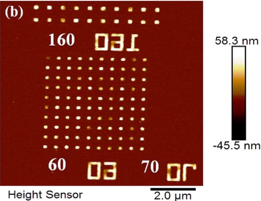
- Surface Potential Investigations of Post Deposition Annealed Er2O3 films by Kelvin Probe Force Microscopy
for Scaled Memory Device Applications
Pawan Kumar, Robin Khosla, Satinder K. Sharma; Surface and Interfaces, vol 4, pp-69-76, (2016); 10.1016/j.surfin.2016.08.003
- Design, development and nano mechanical investigations of a new organic monomer and HfO2 nano-particles
based hybrid resist for EUVL applications
Pulikanti Guruprasad Reddy, Narsimha Mamidi, Pawan Kumar, Satinder K. Sharma, Subrata Ghosh, Kenneth E. Gonsalves, Chullikkattil P. Pradeep; RSC Adv., vol 6, pp-67143-67149, (2016), Impact factor 3.3; 10.1039/C6RA10575K
- Patterning highly ordered arrays of complex nanofeatures through EUV directed polarity switching of
non-chemically amplified photoresist
Subrata Ghosh, V. S. V. Satyanarayana, Bulti Pramanick, Satinder K. Sharma, Chullikkattil P. Pradeep, Israel Morales-Reyes, Nikola Batina, Kenneth E. Gonsalves; Nature, Scientific Reports, vol 6, pp-22664, (2016); 10.1038/srep22664
- Integration of Highly Sensitive Oxygenated Graphene with Aluminum Micro-Interdigitated Electrode Array Based
Molecular Sensor for Detection of Aqueous Fluoride Anions
Mahesh Soni, Tarun Arora, Robin Khosla, Pawan Kumar, Ajay Soni, Satinder K. Sharma, IEEE Sensors Journal, VOL. 16, NO. 6, MARCH 15, (2016), I.P>3.0; 10.1109/JSEN.2015.2505782
- Charge Trapping and Decay Mechanism in Post Deposition Annealed Er2O3 MOS Capacitors by Nanoscopic and
Macroscopic Characterization
Robin Khosla, Pawan Kumar and Satinder K. Sharma; IEEE Transactions On Device and Materials Reliability, Vol. 15, No. 4, December (2015), Impact factor 1.9; 10.1109/TDMR.2015.2498310
- Dual Gate Tunable and High Responsivity Graphene-Based Field Effect Transistors
Mahesh Soni, Satinder Kumar Sharma, Ajay Soni; Macromol. Symp. Soft Materials, 357, pp-12-17, (2015); 10.1002/masy.201400176
- Multilevel Metal-Pb (Zr0.52 Ti0. 48) O3-TiOxNy-Si for Next Generation FeRAM Technology Node
Deepak K. Sharma, Robin Khosla and Satinder K. Sharma; Solid-State Electronics, vol 5, (2015), Impact factor 1.58; 10.1016/j.sse.2015.04.006
- An 8 bit, 100 kS/s, Switch-Capacitor DAC SAR ADC for RFID applications
Ashish Joshi, Sanjeev Manhas, Satinder K. Sharma and S. Dasgupta; Microelectronics Journal, vol 46, pp-453-461, (2015), Impact factor 0.92; 10.1016/j.mejo.2015.03.009
- New Polyoxometalates Containing Hybrid Polymers and Their Potential for Nano-patterning
Vishwanath Kalyani, V. S. V. Satyanarayana,Vikram Singh,Chullikkattil P. Pradeep, Subrata Ghosh, Satinder K. Sharma, Kenneth E. Gonsalves; Chemistry A Chem. Eur. J., vol 21, pp-2250-2258, (2015), Impact Factor: 5.7; 10.1002/chem.201405369
- Effect of electrical stress on Au/Pb (Zr0.52Ti0.48) O3/TiOxNy/Si gate stack for reliability analysis of ferroelectric
field effect transistors
Robin Khosla, Deepak K. Sharma, Kunal Mondal and Satinder K. Sharma; Applied Physics Letters, vol 105, (2014), I.P> 3.59; 10.1063/1.4897952
- Templated Electrochemical Synthesis of Polyaniline/ZnO Coaxial Nanowires with Enhanced Photoluminescence
Neelam Saurakhiya, Satinder K. Sharma, Rudra Kumar, and Ashutosh Sharma; Industrial & Engineering Chemistry Research (I & EC, Research), vol 27, (2014), I.P>2.25; 10.1021/ie500989m
- Performance evaluation of nonchemically amplified negative tone photoresists for e-beam and EUV lithography
Vikram Singh, V.S.V.Satyanarayana, Nikola Batina, Israel Morales Reyes, Satinder K. Sharma, Felipe Kessler, Francine R. Scheffer, Daniel E. Weibel, Subrata Ghosh and Kenneth E. Gonsalves; J. Micro/Nanolith. MEMS MOEMS, Society of Photo-Optical Instrumentation Engineers (SPIE), (2014), Impact factor: 1.20; 10.1117/1.JMM.13.4.04300210
- A hybrid polymeric material bearing a ferrocene based pendant organometallic functionality: synthesis and applications in
nano patterning using EUV lithography
V. S. V. Satyanarayana, Vikram Singh, Vishwanath Kalyani, Chullikkattil P. Pradeep, Satinder Sharma, Subrata Ghosh and Kenneth E. Gonsalves; RSC Advances Journal, RSC Adv., Vol 4, PP-59817, (2014), Impact factor: 3.7; 10.1039/c4ra10648b
- Design and synthesis of novel resist materials for EUVL
V. S. V. Satyanarayana, Vikram Singh, Subrata Ghosh, Satinder Sharma, Kenneth E. Gonsalves; Proc. of SPIE Vol. 9048, 90481W, CCC code:0277-786X/14/$18, (2014); 10.1117/12.2045736
- Tuning of structural, optical, and magnetic properties of ultrathin and thin ZnO nanowire arrays for nano device applications
Satinder K. Sharma, Neelam Saurakhiya, Sumit Barthwal, Rudra Kumar and Ashutosh Sharma; Nanoscale Research Letters, vol 9:122, (2014), I.P> 3.55; 10.1186/1556-276X-9-122
- Organic-Inorganic Hybrid Resists for EUVL
Vikram Singh, Vishwanath Kalyani, V. S. V. Satynarayana, Pradeep Parameswaran, Subrata Ghosh, Satinder K. Sharma, Kenneth E. Gonsalves; Proc. of SPIE Vol. 9051, 90511W,SPIE CCC code: 0277-786X/14/$18, (2014); 10.1117/12.2041907
- A Switch-Capacitor DAC Successive Approximation ADC Using Regulated Clocked Current Mirror
Ashish Joshi, Satinder Sharma, Sanjeev Manhas and S. Dasgupta; International Journal of Electronics and Electrical Engineering (IJEEE), Vol.2, No.1, (2014); 10.12720/ijeee.2.1.50-55
- Novel non-Chemical Amplified (n-CARs) Negative Resists for EUVL
Vikram Singh, V. S. V. Satyanarayana, Satinder K. Sharma, Subrata Ghosh, Kenneth E. Gonsalves; Advances in Patterning Materials and Processes Proc. of SPIE Vol. 9051, 905106, SPIE CCC code: 0277-786X/14/$18, (2014); 10.1117/12.2041183
- Towards Novel non-Chemically Amplified (n-CARS) Negative Resists for Electron Beam Lithography Applications
Vikram Singh, V. S. V. Satyanarayana, Satinder K. Sharma, Subrata Ghosh, Kenneth E. Gonsalves; J. Mater. Chem. C, vol 2, pp-2118-2122, (2014), Impact factor 6.2; 10.1039/c3tc31826e
- Optimization of processing parameters and metrology for novel NCA negative resist for NGL
Vikram Singh, V. S. V. Satyanarayana, Felipe Kessler, Francine R. Scheffer, Daniel E. Weibel, Satinder K. Sharma, Subrata Ghosh, Kenneth E. Gonsalves; Proc. of SPIE Vol. 9048, 90481Y, SPIE CCC code: 0277-786X/14/$18, (2014). DOI: 10.1117/12.2045882
- PZT-PDMS composite for active damping of vibrations
Satinder K. Sharma, Himani Gaur, Manish Kulkarni, Ganesh Patil, Bishakh Bhattacharya, Ashutosh Sharma; Composites Science and Technology, vol 77, pp-42-51, (2013), Impact factor 3.9; 10.1016/j.compscitech.2013.01.004
- PECVD based silicon oxynitride thin films for nano photonic on chip interconnects applications
Satinder K. Sharma, Sumit Barthwal, Vikram Singh, Anuj Kumar, Prabhat K. Dwivedi, B. Prasad, Dinesh Kumar; Micron, vol 44, pp-339-346, (2013), Impact factor 2.1; 10.1016/j.micron.2012.08.006
- Antimicrobial Properties of Electro-ChemicallyStabilized Organo-Metallic Thin
Kumud Kant Awasthi, Anjali Awasthi, Kamakshi, Narain Bhoot, P. J.John, Satinder K. Sharma, and Kamlendra Awasthi; Advanced Electrochemistry, vol 6, pp-1-6, (2013), Impact factor 1.2; 10.1166/adel.2013.1013
- Chalcogenide Glass Photoresists for Grayscale Patterning
Prabhat K. Dwivedi, Amritha Rammohan,Satinder K. Sharma, Ashutosh Sharma; AIP Conference Proceedings Vol.1349, 555 (2011);, Impact factor 1.8; 10.1063/1.3605979
- Surface disordering and its correlations with properties in argon implanted CR-39 polymer
Nidhi Shekhawat, Sanjeev Aggarwal,Annu Sharma, Satinder K. Sharma, S. K. Deshpande, and K. G. M. Nair; Journal of Applied Physics, vol 109, pp-083513, (2011), I.P>2.8; 10.1063/1.3573480
- Study of Rapid Thermal Annealing on Ultra Thin High-K HfO2 Films Properties for nano Scaled MOSFET Technology
Vikram Singh, Satinder K.Sharma, Dinesh Kumar , R.K. Nahar; Microelectronics Engineering B, (2011), Impact factor 1.7; 10.1016/j.mee.2011.09.005
- Frequency Dependence Studies on the Interface Trap Density and Series Resistance of HfO2 Gate Dielectric
Deposited on Si Substrate: Before and After 50MeV Li3+ Ions Irradiation
Vikram Singh,N.Shashank, Satinder K. Sharma, Dinesh Kumar, R.K. Nahar; Nuclear Instruments and Methods in Physics Research B., (2011), Impact factor 1.2; 10.1016/j.nimb.2011.08.025
- Large scale synthesis of polyaniline nanowires and their characterization
Sanjeev Kumar and Satinder K. Sharma; Journal of Materials Science: Materials in Electronics, I.P> 2.2, (2011); 10.1007/s10854-011-0583-7
- High-k Dielectric Stacks Charge Trapping for CMOS Technology
Satinder K. Sharma, B.Prasad and Dinesh Kumar; Material Science and Engineering B, vol 166, pp-170-173, Impact factor 2.7, (2010); 10.1016/j.mseb.2009.11.002
- One Step Electrodeposition of High Aspect Ratio n-type ZnO Nanowire Arrays
Satinder K. Sharma, Amritha Rammohan and Ashutosh Sharma; Journal of Colloidal and Interfacial Science, (2010), Impact factor 3.5; 10.1016/j.jcis.2009.12.026
- Stability and Dewetting of Metal Nanoparticles Filled Thin Polymer Films: Control of Instability Length scale and Dynamics
Rabibrata Mukherjee, Soma Das, Anindya Das, Satinder K. Sharma, Arup K. Raychaudhuri and Ashutosh Sharma; ACS NANO, Impact factor 10.0, (2010); 10.1021/nn901912d
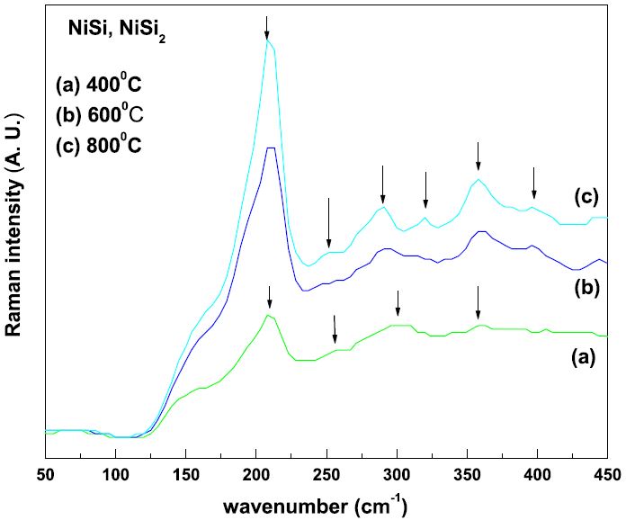
- Nickel silicide formation by electroless technique for ULSI technology
Anuj Kumar, Mukesh Kumar, Amanpal Singh, Satinder Kumar, Dinesh Kumar; Microelectronic Engineering, vol 87, pp-286-289, (2010), I.P> 2.3; 10.1016/j.mee.2009.07.021
- Changes in Structural and Optical Properties of Polycarbonate Induced by Ag+ Ion Implantation
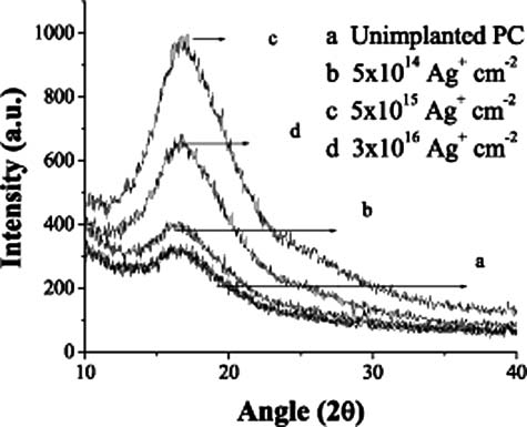
Suman Bahniwal, Annu Sharma, Sanjeev Aggarwal, S.K. Deshpande, Satinder K. Sharma, K.G.M.Nair; Journal of Macromolecular Science, Part B, vol 49, no. 2, pp-259-268, (2010), Impact factor 1.0; 10.1080/00222340903352252
- Large scale synthesis of cadmium selenide nanowires using template synthesis technique and their Characterization
Sanjeev Kumara, Vijay Kumar, Satinder K. Sharma, S.K. Sharma, S.K. Chakarvarti; Superlattices and Microstructures, pp-1-9, (2010), I.P> 2.0; 10.1016/j.spmi.2010.03.008
- Low-temperature synthesis and characterization of cadmium sulphide nanowires grown using simple chemical
reaction through the pores in an alumina template
Sanjeev Kumar and Satinder K Sharma; IOP Publishing Phys. Scr., vol. 82, 000000, 4pp, (2010), Impact factor 1.0; 10.1088/0031-8949/82/02/025801
- Alteration of Gate Oxides Thickness for SOC Level Integration
Satinder K. Sharma, B. Prasad, Dinesh Kumar and Rajkumar; Materials Science in Semiconductor Processing, vol 12, pp-99, (2009), I.P>3.0; 10.1016/j.mssp.2009.08.003
- Growth and Characterization of Large -Scale Uniform Zinc Sulfide Nanowires by Simple Chemical Reaction Technique
Sanjeev Kumar, Satinder K. Sharma; Superlattices & Microstructures, (2009), I.P>2.0; 10.1016/j.spmi.2009.08.008
- Multiple thickness gate oxides with fluorine implantation for system on chip applications
Satinder K. Sharma, B. Prasad, Dinesh Kumar, RajKumar; Vacuum, vol. 83, pp-1359, (2009), I.P>2.9; 10.1016/j.vacuum.2009.04.045
- Structural and optical characterization of ZnO thin films deposited by sol-gel method
A.Singh, A. Kumar, N.Suri, Satinder K. Sharma, M.Kumar, P.K.Khanna, D.Kumar; Journal of Optoelectronics and Advanced Materials (JOM), pp-790-793, (2009), I.P>0.9;
- Surface topography and morphology characterization of PIII irradiated silicon surface
Satinder K. Sharma and Sumit Barthwal; Applied Surface Science, 17552, pp-1-6, (2008),I.P>6; 10.1016/j.apsusc.2008.07.129
2026
2023
2022
2021
2020
2019
2018
2017
2016
2015
2014
2013-2012
DOI: 10.1063/1.3605979
2011
2010
2009-2008
(Kindly refresh page if this message is visible: "Requested article is not found in IHub.")
List of Upcoming Journals
- Incorporation of organometallic Tin into multi-functionally decorated macromolecular network
Midathala Yogesh, Mohamad. G. Moinuddin, Lalit D. Khillare, Srinivas Chinthalapalli, Subrata Ghosh, Satinder K. Sharma and Kenneth Gonsalves. communicated to European Polymer Journal. - Low Voltage Operation and High Mobility with Nitrogen Functionalized Reduced Graphene Oxide based Organic Transistors for
Flexible Electronic Circuits
Mahesh Soni, Ajay Soni, Satinder K. Sharma; communicated to IEEE Transaction Nanotechnology. - Self-calibrated and Digitally Assisted Comparator with Supplementary LSB Generation
Ashish Joshi, Hitesh Shrimali, and Satinder K. Sharma; comminucated in IET Electronics Letters, 2019. - Z-axis MEMS Accelerometers using SU-8, PolySi, Si3N4 and SiC based structural materials
Mandeep Jangra, Robin Khosla, and Satinder K. Sharma; communicated to IEEE Sensors Journal. - Ferroelectric Materials: An Ultimate Solution for Next Generation Universal Memories
Robin Khosla and Satinder K. Sharma; communicated to Journal of Materials Research Bulletin. - Highly Sensitive SERS Sensors Based on Ag coated Self Assembled Colloidal Crystals for Detection of Contaminants in Water
Pawan Kumar, Mahesh Soni, Tarun Arora, Robin Khosla and Satinder K. Sharma; communicated to Advanced Materials Letters.
List of Book Chapters
- Monograph; Nanostructured Zinc Oxide Synthesis, Properties and Applications, 1st Edition - August 10, 2021, Editor: Kamlendra Awasthi, Language: English, Paperback ISBN: 9780128189009, eBook ISBN: 9780128189016 "Diverse morphology zinc oxide films formulations and characterizations" by Shivani Sharma and Satinder K. Sharma.
List of Published International/National Conferences
- Design and Simulation of Capacitive Z-axis MEMS Accelerometers using SU-8, PolySi, Si 3 N 4, and SiC-based structural materials
Satinder K. Sharma, Mandeep Jangra, Dhairya Singh Arya, Robin Khosla. IEEE-ICEE 2020, 5th International Conference on Emerging Electronics, Hosted by- Indian Institute of Technology Delhi, India from 26th - 28th Nov. (2020) 10.1109/ICEE50728.2020.9776817 - Highly Sensitive Polymer Micro-Mesh for Measurement of Vacuum Packaged MEMS Devices
Satinder K. Sharma, Manu Garg, Dhairya S. Arya, Mohamad G. Moinuddin, Pushpapraj Singh. PIEEE-ICEE 2020, 5th International Conference on Emerging Electronics, Hosted by- Indian Institute of Technology Delhi, India from 26th - 28th Nov. (2020) 10.1109/ICEE50728.2020.9776980 - Focusing on nanoparticles based photomultiplier in n-CARs
Satinder K. Sharma, Mohamad G. Moinuddin, Midathala Yogesh, Shivani Sharma, Manoj Sahani, Subrata Ghosh, Kenneth E. Gonsalves; Proc. SPIE 11326, Advances in Patterning Materials and Processes XXXVII, 113261C, San Jose, California, USA, 23 March (2020). 10.1117/12.2552190 - All new nickel based Metal Core Organic Cluster (MCOC) resist for N7+ node patterning
Satinder K. Sharma,Rudra Kumar, Manvendra Chauhan, Mohamad G. Moinuddin, Jerome Peter, Subrata Ghosh, Chullikkattil P. Pradeep, Kenneth E. Gonsalves; Proc. SPIE 11326, Advances in Patterning Materials and Processes XXXVII, 1132604, San Jose, California, USA, 26 March (2020). 10.1117/12.2552189 - The Capacitively Coupled Chopper Stabilized Amplifier with a DTPA based Demodulator
A. Joshi, H. Shrimali and S. K. Sharma; IEEE International Symposium on Circuits and Systems (ISCAS), Florence, pp. 1-5, (2018). 10.1109/ISCAS.2018.8351188 - Electrically Controlled Magnetic Tunnel Junctions for Next Generation Magnetic Non-Volatile Memory Applications
Moinuddin, M.G. Srinivasan, Srikant, Sharma, Satinder K.; International workshop on NANO/MICRO 2D-3D Fabrication, Manufacturing of Electronic - Biomedical Devices & Applications, (IWNEBD-2018), IIT Mandi, 31 Oct. - 2 Nov., (2018)., - Evaluation of High Resolution & Sensitivity of n-CAR Hybrid Resist for Sub-16nm or Below Technology Node
Satinder K. Sharma, Mohamad Ghulam Moinuddin, Pulikanti Guruprasad Reddy, Chullikkattil P. Pradeep, Subrata Ghosh, and Kenneth E. Gonsalves; SPIE Advanced Lithography 2018, on 21 - 25 February 2018 at San Jose, California United States (USA), (2018). 10.1117/12.2297565 - Helium Ion Active Novel Hybrid n-CAR Resist for Sub-10 nm Patterning Applications
Satinder K. Sharma, Pulikanti Guruprasad Reddy, Mohamad Ghulam Moinuddin, Subrata Ghosh, Chullikkattil P. Pradeep, and Kenneth E. Gonsalves; Symposium: SPIE Advanced Lithography 2018, at San Jose, California United States (USA), 2018. 10.1117/12.2297537 - Photoresist development for sub-22 nm node technology: Polyarylenesulfonium salt as negative tone resist for
electron beam lithography
Mohamad Ghulam Moinuddin, Pulikanti Guruprasad Reddy, Satinder K Sharma , Chullikkattil P. Pradeep, Subrata Ghosh, and Kenneth E. Gonsalves; National Conference on Complex Engineering Systems of National Importance: Current Trends & Future Perspective, INAC-03 2017 Proceedings (554-557) Organised by ISSE - Chandigarh Chapter & Semi-Conductor Laboratory, Department of Space, Indian School of Business, Chandigarh, October 12-13, 2017. (Awarded with best paper presentation 3rd prize) - Impact of Metal Electrodes on MFIS Structure Performance for NextGeneration FeRAM Applications
Robin Khosla, and Satinder K. Sharma; National Conference on Complex Engineering Systems of National Importance: Current Trends & Future Perspective, Organised by ISSE - Chandigarh Chapter & Semi-Conductor Laboratory, Department of Space, Indian School of Business, Chandigarh, october 12-13, 2017. - Capacitively Coupled Chopper Stabilized Instrumentation Amplifier for a Biomedical Data Acquisition
System in 180 nm CMOS
Ashish Joshi, Hitesh Shrimali and Satinder K Sharma; National Conference on Complex Engineering Systems of National Importance: Current Trends & Future Perspective, Organised by ISSE - Chandigarh Chapter & Semi-Conductor Laboratory, Department of Space, Indian School of Business, Chandigarh, October12-13, 2017. - The Pole-zero Doublet: a Cascode Operational Amplifier with Cross Coupled Capacitor
Ashish Joshi, Indu Yadav, Satinder K. Sharma and Hitesh Shrimali; MWSCAS Abu Dhabi 2016; IEEE 59th International Midwest Symposium on Circuits and Systems 16-19 October, Hotel Fairmont Bab Al Bahr, Abu Dhabi, United Arab Emirates, 2016. 10.1109/MWSCAS.2016.7869985 - Design and development of low-activation energy based n-CARs for next-generation EUV lithography
Satinder K. Sharma, Narsimha Mamidi, Rakhi Pramanick, Pawan Kumar, Subrata Ghosh, Chullikkattil P. Pradeep and Kenneth E. Gonsalves; Symposium: SPIE Advanced Lithography 2016, held on 21 - 25 February 2016 at San Jose, California United States (USA), 2016. 10.1016/j.mee.2016.07.017 - Highly Sensitive SERS Sensor Based on Ag coated Self Assembled Colloidal Crystals for Detection of Contaminants present in Water
Pawan Kumar, Mahesh Soni, Tarun Arora, Robin Khosla and Satinder K. Sharma; International Conference on Materials Science & Technology 2016 (A Global platform for high-tech materials) held on 01 -04 March, 2016 at the Conference Centre, University of Delhi, India, 2016. - GO/�-IDEs/p-Si Based Real Time Sensors for F- Detection in Natural Drinking Water
Mahesh Soni, Tarun Arora, Pawan Kumar, Ajay Soni, Satinder K. Sharma; 1st IEEE International Symposium on Nanoelectronic and Information System (IEEE-iNIS), 21- 23 December 2015, Indore, India, 2015. 10.1109/iNIS.2015.14 - 2D Colloidal Crystals based SERS Sensors for NH3 Detection
Pawan Kumar, Mahesh Soni, Tarun Arora, Satinder K. Sharma; 1st IEEE International Symposium on Nanoelectronic and Information System (IEEE-iNIS), 21- 23 December 2015, Indore India (2015) DOI: 10.1109/iNIS.2015.53 10.1109/iNIS.2015.53 - High performance Au/PZT/TiOxNy/Si MFIS structure for next generation ferroelectric memory applications
Deepak K. Sharma, Robin Khosla and Satinder K. Sharma; International Conference on Condensed Matter Physics, ICCMP, Himachal Pradesh University-Shimla, 2014. 10.1063/1.4915377 - Charge carrier controlling in Dual Gated Graphene Based Field Effect Transistors
Mahesh Soni, Satinder K. Sharma, Ajay Soni; International Conference on Soft Materials October, 06-10, ICSM 2014 in Jaipur India, 2014. - DAC Successive Approximation ADC Using Clocked Current Mirror
Ashish Joshi, Satinder Sharma, Sanjeev Manhas and S. Dasgupta; International Conference on Advances in Electronics Engineering, Feb: 19-20, Singapore, 2014. doi: 10.12720/ijeee.2.1.50-55 - Optimization of processing parameters and metrology for novel NCA negative resist for NGL
Vikram Singh, V. S. V. Satyanarayana, Felipe Kessler, Francine R. Scheffer, Daniel E. Weibel, Satinder K. Sharma, Subrata Ghosh, Kenneth E. Gonsalves; SPIE Advanced Lithography Symposium-2014, Extreme Ultaviolet (EUV) Lithography V, SPIE paper no, 9048-69, 2014. 10.1117/12.2045882 - Design and synthesis of novel resist materials for EUVL
V. S. V. Satyanarayana, Vikram Singh, Subrata Ghosh, Satinder Sharma, Kenneth E. Gonsalves; SPIE Advanced Lithography Symposium-2014, Extreme Ultaviolet (EUV) Lithography V, SPIE paper no, 9048-67, 2014. >10.1117/12.2045736 - Organic-Inorganic Hybrid Resists for EUVL
Vikram Singh, Vishwanath Kalyani, V. S. V. Satynarayana, Pradeep Parameswaran, Subrata Ghosh, Satinder K. Sharma, Kenneth E. Gonsalves; SPIE Advanced Lithography Symposium-2014, Advances in Patterning Materials and Processes XXXI, SPIE paper no, 9051-71, 2014. 10.1039/C7QM00343A - Novel non-Chemical Amplified (n-CARs) Negative Resists for EUVL
Vikram Singh, V. S. V. Satyanarayana, Satinder K. Sharma, Subrata Ghosh, Kenneth E. Gonsalves; SPIE Advanced Lithography Symposium-2014, Advances in Patterning Materials and Processes XXXI, SPIE paper no, 9051-5, 2014. 10.1117/12.2041183 - Novel Non-Chemically Amplified (n-CARs) Resists for Next Generation Lithography (NGL) Applications
Vikram Singh, V. S. V. Satyanarayana, Vishwanath Kalyani, Satinder K. Sharma, Subrata Ghosh, Chullikkattil P. Pradeep and Kenneth E. Gonsalves; ICON-2014, Theme 06: Nanolithography / Microfluids:- Abstract No.:- 17 ; Poster ID:- P-12 (T-6)., at Chandigarh, India, on March 3-5, 2014. (Received the best poster award sponsored by RSC) - Radial hetrojunction formation of ZnO-Polyaniline coaxial nanowires via electrochemical route
Neelam Saurakhiya, Satinder Kumar Sharma, Ashutosh Sharma; International Conference on Nanoscience and Technology (ICONSAT - 2012) January 20 to 23, at Hyderabad, India, 2012. - Ultrathin HfO2 based CMOS for space application
Vikram Singh, Satinder K. Sharma, R.K. Nahar , Dinesh Kumar; International conference on nano materials and Nanotechnology,18-23 December, at University of Delhi, India, 2011. - Effects of Post-Deposition Annealing on the Material and Electrical Characteristics of Sputtered Ultrathin HfO2 Film on Silicon
Vikram Singh, Satinder K. Sharma, R.K. Nahar , Dinesh Kumar; 16th International Workshop on The Physics of Semi Conductor Devices, at Indian Institute of Technology-Kanpur, India, 2011. - Chalcogenide Glass Photoresists for Grayscale Patterning
Prabhat K. Dwivedi, Satinder K. Sharma, Amritha Rammohan and Ashutosh Sharma; 55th DAE Solid State Physics Symposium, India, 2010. - Polyaniline 1D Nanostructures film formation by electrochemical deposition for Biomedical Applications
Neelam Saurakhiya, Satinder K. Sharma and Ashutosh Sharma; International Conference on Nano Science and Technology(ICONSAT), held at IIT Bombay, Mumbai, India, 17-20,February, 2010. - Templated electrodeposition of ZnO nanowires array for bio sensing application
Satinder K. Sharma, Amritha Rammohan and Ashutosh Sharma; Golden Jublilee Symposium on fabrication at small scale and INDO-US conference on fabrionics, organized by IIT -Kanpur, U.P. India, 9-12 December, 2009. - Synthesis and Characterisation of Erbium Nano Particle doped High k Dielectric Thin film for Novel device Applications
Vikram Singh, Satinder Kumar, Dinesh Kumar, R.K. Nahar; XI international conference on advanced materials (ICAM-09) at Rio de Janeiro Brazil, Sept 2009. - Raman study on NiSi formation by Electroless for ULSI technology
Anuj Kumar, Mukesh Kumar, Amanpal Singh, Satinder Kumar, B. Parsad and D. Kumar; Ist Rashtreeya Yuva Vaigyanik Sammelan organized by National Institute of Technology, Kurukshetra, Haryana, India, 28-30 November, 2008. - The evolution of phase transformation during annealing of electroless Ni-Co-P alloy thin Film
Anuj Kumar, Amanpal Singh, Satinder Kumar, Mukesh Kumar, B. Prasad and Dinesh Kumar; National Conference on Photonics & Material Science, Guru Jambheshwer University, Hisar, Haryana, India, October 24-25, 2008. - Deposition and characterization of electroless Ni-Co-P alloy thin film
Anuj Kumar, Amanpal Singh, Satinder Kumar, Mukesh Kumar, B. Prasad and D. Kumar; Gurukula Kangri Vishwavidyalaya Haridwar India, 16-18 October, 2008. - Experimental Determination of Threshold Voltage Shift in Submicron Devices
Satinder K. Sharma, Anuj Kumar, B. Prasad and Dinesh Kumar; 52nd DAE Solid State Physics Symposium, Department of Studies in Physics, University of Mysore, MYSORE, from 27-31 December 2007. - Electrical Characteristics of SiOxNy/HfO2 Stack Structure for High Performance Sub- micron CMOS Devices
Satinder K. Sharma, B. Prasad and Dinesh Kumar; (INCCOM-6), International Conference on Future Trends in Composite Materials and Processing, at Indian Institute of Kanpur (U.P) from December 12-14, 2007. - Role of +19F Implanted to Grow Multiple Gate Oxides for Nano-CMOS Technology
Satinder K. Sharma, B. Prasad, Dinesh Kumar and Rajkumar; International Conference on Micro and Nanotechnology held at University of Mouloud Mammeri Of TIZI-OUZOU, ALGERIA, November 19-23, 2006. http://aphysrev.ictp.it/index.php/aphysrev/article/viewArticle/247. - Effectof Post Metallization Annealing on hysterisis of C-V and G-V characteristics of PECVD deposited silicon oxynitride thin films
Satinder K. Sharma,Dinesh Kumar and B.Prasad; National Conference held at Kurukshetra University, Sep. 2006. - High Frequency Simultaneous Measurement for Rapid Characterization of MIS Structure
Satinder K. Sharma, Anil Dutt,B. Prasad, Dinesh Kumar and P.J.George; National Conference On Recent Advances in Process Control & Instrumentation Engineering held at Kurukshetra University, February 23-25, 2006. - Impact of Post-metallization annealing on the Fluorinated Ultra Thin Gate Oxide in Submicron MOS Devices
Satinder K. Sharma, Rajkumar, B. Prasad, Dinesh Kumar and P.J.George; Indian Microelectronics Society Conference held at Kurukshetra University, February 17-18, 2006. - Application of Plasma Immersion Ion Implantation Technique for Oxynitride Growth as a Gate Dielectric in Sub Micron MOS Devices
Satinder K. Sharma,B. Prasad, Dinesh Kumar and P.J.George; National Conference on Materials and Their Applications held at Kurukshetra University, 2004. - Silicon Oxynitride-Future Gate Material
Satinder K. Sharma, B. Prasad, Dinesh Kumar and P.J.George; National Conference on Materials and Related Technologies held at Thapar Institute of Engineering and Technology, Patiala, ep19-20, 2003. (Published as special proceedings)
2020
2018
2017
2016-2015
2014
2012-2010
2009-2007
2006-2003
Device Engineering Lab (DEL) Research Group & Members
- Mr. Pankaj Kumar
Year of Joining: 2022 (PhD)
Research Area: Piezoelectric Sensors
Research Scholar, SCEE, IIT Mandi - Mr. Sachin
Year of Joining: 2023 (PhD)
Research Area:
Research Scholar, SCEE, IIT Mandi - Mr. Naresh Sharma
Year of Joining: 2023 (PhD)
Research Area:
Research Scholar, SCEE, IIT Mandi
Present Graduate Students
- Dr. Robin Khosla
Year of Graduation: 2017 (Doctor of Philosophy)
Thesis: Alternate High-k Dielectrics for Next-Generation CMOS Logic and Memory Technology
Current Position: Assistant Professor, Indian Institute of Technology (IIT)-Mandi, India
LinkedIn, Google Scholar, Research Gate
- Dr. Mahesh Soni
Year of Graduation: 2018 (Doctor of Philosophy)
Thesis: Graphene and Derivatives based Scaled Electronic and Memory Devices for Next Generation Technology
Current Position: Post Doctoral Fellow, Lancaster University, Lancashire, United Kingdom
LinkedIn, Google Scholar, Research Gate
- Dr. Ashish Joshi
Year of graduation: 2020 (Doctor of Philosophy)
Thesis: Multivalent Energy-Efficient CMOS Amplifiers and Data Converters for Signal Processing Applications LinkedIn, Google Scholar
- Dr. Shivani Sharma
Year of graduation: 2020 (Doctor of Philosophy)
Thesis: High-k Dielectrics for two dimensional Multilayer Hafnium Disulfide based Interdigitated Electrode based Field Effect Transistors: Next Generation Technology
Current Position: Assistant Professor, Jaypee Institute of Information Technology, UP, India
LinkedIn Google Scholar, Research Gate
- Dr. Mohamad Ghulam Moinuddin
Year of graduation: 2022 (PhD)
Research Area: CMOS compatible Spintronics devices and Nano Lithography
Current Position: Systems on Silicon Manufacturing Company Pte Ltd (SSMC), Singapore.,
LinkedIn, Research Gate
- Dr. Sumit Choudhary
Year of graduation: 2023 (PhD)
Research Area: Germanium based FETs
Current Position: Assistant Professor,Department of VLSI Design & Technology, Gurugram University
Google Scholar
- Dr. Manoj Kumar Yadav
Year of Joining: 2017 (PhD)
Research Area: Ga2O3 based power semiconductor devices.
Research Scholar, Indian Institute of Technology Mandi, Kamand
Research Gate
- Dr. Prachi Gupta
Year of Joining: 2017 (PhD)
Research Area: CMOS Logic devices, High-k dielectrics, 2D Materials based FETs
Research Scholar, SCEE, IIT Mandi
LinkedIn, Google Scholar, Research Gate
- Dr. Arnab Mondal
Year of Joining: 2019 (PhD)
Research Area:
Research Scholar, Indian Institute of Technology Mandi, Kamand-IIT Mandi
- Dr. Manvender Singh Chauhan
Year of Joining: 2019 (PhD)
Research Area: Photoresist, Helium Ion Beam Lithography
Research Scholar, SCEE, IIT Mandi
Past Graduate Students
- Dr. Rudra Kumar
Year of completion: 2020 (National Post Doctoral Fellow)
Research Area: Electrochemistry, Energy Storage Devices, Photoresist Devices
Current Position: Assistant Professor, Tecnol�gico de Monterrey, Mexico
Google Scholar, Research Gate
- Dr. Jerome Peter
Year of completion: 2019 (National Post Doctoral Fellow)
Research Area: Synthesis of Inorganic hybrid polymeric materials for lithographic applications
Current Position: Post-Doctoral Researcher, Pusan National University, Busan, South Korea
Google Scholar, Research Gate
- Dr. Subhasis Das
Year of completion: 2019 (National Post Doctoral Fellow)
Research Area: Gas Sensors, 2D Materials
Current Position: Research Associate, Department of Physics, Institute for Nanoscience and Engineeing, University of Arkansas, Fayetteville
LinkedIn, Google Scholar, Research Gate
National Post Doctoral Fellow
- Mr. Rahul Sharma
Year of Graduation: 2022 (Master of Science by Research)
Research Area:
Research Scholar, Indian Institute of Technology Mandi, Kamand
- Mr. Saswath T
Year of Graduation: 2020 (Master of Technology with specialization in VLSI)
Thesis: Design of Variable gain low noise capaciatnce to voltage converter for vibratory gyroscope in space applications
LinkedIn - Mr. Diwakar Chauhan (co-supervised)
Year of Graduation: 2019 (Master of Technology)
Thesis: A low cost Reverse Electrowetting on dielectric (REWOD) System
Current Position: Research Scholar, Indian Institute of Technology Mandi, Kamand - Mr. Shivendra Rathaur
Year of Graduation: 2018 (Master of Technology with specialization in VLSI)
Thesis: Metal/Ferroelectric/Insulator/Semiconductor MFIS structure for Ferroelectric Memory Applications
Current Position: Research Scholar, Indian Institute of Technology Delhi, Hauz Khas, Delhi - Mr. Deepak Sharma
Year of Graduation: 2014 (Master of Science by Research)
Thesis: High-k TiOxNy based MFIS Structure for Next Generation FeRAM Applications
Current Position: Scientist , Laboratory for Electro-Optics Systems (LEOS), ISRO, Bangalore, Govt. of India
Google Scholar
Past Masters Students
- Sachin
Year of Graduation: ...... Master of Science (Electronics)
Thesis: ()
Institute: Kurukshetra University - Priyanka Bedwal
Year of Graduation: ...... Master of Science (Electronics)
Thesis: ()
Institute: Kurukshetra University - Ms. Jyoti Yadav
Year of Graduation: 2018 Master of Science (Electronics)
Thesis: High performance flexible PVDF Nanogenertor for portable electronic device Application.
Institute: Kurukshetra University - Mr. Nidhin S. Babu
Year of Graduation: 2018 Master of Science (Electronics)
Thesis: Sn. nanoparticles doped TiO2 nanofibres for high performance UV photodetectors
Institute: Kurukshetra University - Ms. Amrita Kaur
Year of Graduation: 2017 (M.Tech)
Thesis: Cordic Processor for performing Trignomtric Functions
Institute: Kurukshetra University - Mr. Atul Grewal
Year of Graduation: 2017 (M.Tech)
Thesis: Design of a 128Kb SRAM using 180nm Technology
Institute: Kurukshetra University - Ms. Chanchal Soni
Year of Graduation: 2017 Master of Science (Electronics)
Thesis: All Carbon based strain sensor.
Institute: Kurukshetra University - Mr. Mandeep Kumar
Year of Graduation: 2017 Master of Science (Electronics)
Thesis: MEMS based gyroscope
Institute: Kurukshetra University
Masters Dissetation Supervised
- Ms. Smriti Verma
Project:
Institute: - Ms. Surbhi
Project: Thin film study of PVDF.
Institute: Shri Mata Vaishno Devi University, Katra - Mr. Suja
Project: Modified synthesis of rGo
Institute: - Mr. Sidharth
Project:
Institute: - Ms. Sunita
Project: Traffic Light controller.
Institute: Baddi University of Emerging Sci. & Tech. - Mr. Ajit
Project: Solution compatible of SU8 photoresist
Institute: National institute of technology, Hamirpur, (H.P)
B.tech Interns Supervised
Professional Activities & Memberships of Professional Societies & Invited lectures
- Fellow Member, The Institution of Electronics and Telecommunication Engineers (IETE), F500897, 2018.
- Member, Photoresist Research Group.
- International Visit "SPIE Advanced Lithography 2020", 23 - 27 February 2020, San Jose, California, United States.
- International Visit "2nd ELENA: Low energy ELEctron driven chemistry for the advantage of emerging NAno-fabrication methods" at Interuniversity Microelectronics Centre (IMEC), September 4th - 6th, 2019, Leuven, Belgium.
- Invited talk, "2nd International Conference on Soft Materials" (ICSM 2016), 12-16 December 2016, Jaipur, India.
- Invited talk, National Conference on "Advances in Basic & Applied Sciences" (ABAS-2017), 07- 08 April, 2017 , Hamirpur, India.
Research Project/Awards
- Next Generation, Cutting-Edge Indigenous EUVL Resists Technology For Semiconductor Industry
Technology System Development Program (TSDP), Department of Science & Technology (DST), Govt. of India, New Delhi,Principal Investigator (PI), 91 Lakhs, 2016-2020. - Special Manpower Development Programme for Chips to System Design (SMDP)
Department of Electronics & Information Technology 6, CGO Complex, New Delhi -110 003, Co-Investigator (Co-PI), 70 Lakhs, 2015-2020. - Tailoring the nanoscale properties of Graphene and its derivatives via strain engineering for next generation
nanoelectronics devices
Department of Science & Technology (DST), (Nanomission), Govt. of India, New Delhi, Co-Investigator (Co-PI), 47 Lakhs, 2019-2022. - Design and fabrication of an interface ASIC for a vibratory gyroscope sensor application
Indian Space & Research Organization (ISRO),Dept. of Space, Govt. of India, Inertial Systems Unit (IISU), Vattiyoorkaavu, Thiruvananthapuram, 695013, Principal Investigator (PI); 49 Lakhs, 2018-2020. - Low-Temperature Epitaxial Growth of High Mobility "Ge1-xSnx" Channel Materialfor "Pt/TiN/high- k/GeOXNY/Ge1-XSnX/Ge/Si" Transistor to the
Integration of Next Generation CMOS and Optoelectronics Devices on Cost Effective Si Platform
Department of Science and Technology (DST) Govt. of India, New Delhi & German Academic Exchange Service (DAAD), Germany, Principal Investigator (PI) from India; 80 Lakhs, 2018-2020. - Indigenous Photoresists Technology for Semiconductor Industries: Impact on Indian Economy,
Skilled Manpower Development and Employment Possibility
Ministry of Human Resource Development (MHRD) (under Uchhatar Avishkar Yojana (UAY) scheme), Govt. of India, New Delhi, Co-Investigator (Co-PI), 239 Lakhs, 2016-2019. - Radiation Impact on SiC based Devices for Space Applications
Indian Institute of Technology (IIT) - Mandi (Himachal Pradesh)-175001 (Under Seed Grant Program), Principal Investigator (PI), 10 Lakhs, 2013-2017. - Non Chemically Amplified Resists for EUVL at the 10 nm Node and Beyond
Intel, Semiconductor Research Corporation, 1101 Slater Road, Brighton Hall, Suite 120, Durham, NC 27703, P.O. Box 12053, Research Triangle Park, NC-27709-2053, Co-Investigator (Co-PI), 250 Lakhs, 2012-2016. - Photo Catalytic treatment of wastewater for removal of AZO dyes; using rGO-TiO2 based cost effective composite technology
Himachal Pradesh Sate Council for Science ,Technology Enviroment (HIMCOST), Shimla, Principal Investigator (PI), 6 Lakhs. - Surface Plasmon Based Flexible Colloidal Crystal Sensors
DST Fast Track Young Scientist, Engineering Section from the Department of Science and Technology (DST), New Delhi, 2012-2015. - Dye Sensitized Hybrid Solar Cells with Up-Conversion Nanostructures with Enhanced Efficiency
PAN IIT-DST, Solar Energy Research Initiative from the Department of Science and Technology (DST), New Delhi, 2012-2014.
Employment Experience
- Professor, in School of Computing and Electrical Engineering (SCEE) at Indian Institute of Technology (IIT)- Mandi, MANDI-175075, Himachal Pradesh, (India). 2021-Continuing Till Date.
- Associate Professor, in School of Computing and Electrical Engineering (SCEE) at Indian Institute of Technology (IIT)- Mandi, MANDI-175075,Himachal Pradesh, (India), 2016-2021.
- Visiting Faculty, , Institute of Semiconductor Electronics (IHT), Stuttgart University, Stuttgart, Germany (BMBF Sponsored TU9 Faculty Exchange Program), 2014-2015,
- Assistant Professor in School of Computing and Electrical Engineering (SCEE) at Indian Institute of Technology (IIT)-Mandi, Himachal Pradesh, (India), 2012-2016.
- Assistant Professor in Electronics and Microelectronics Division at Indian Institute of Information Technology-(IIIT)-Allahabad, (India), 2010-2012.
- Research Scientist, in Department of Science & Technology (DST) Unit on Nano-science & Nanoelectronics, at Indian Institute of Technology (IIT)- Kanpur, (U.P), India.2007-2010.
Education
- Post Doctoral (PDF) in Nano-Science and Nanotechnology (DST Unit on Nanosciences) at Indian Institute of Technology (IIT)-Kanpur, 2007-2010.
- Doctor of Philosophy (Ph.D.) in VLSI Technology from Electronics Science Department, Kurukshetra University, Kurukshetra,2002-2007.
- Master in Science (M.Sc.) Physics (Electronics Science) from department of Physics, Himachal Pradesh University, Shimla, 2000-2002.
- Bachelor of Science (B.Sc.) Physics, Mathematics and Chemistry, 2000.
Open Positions in Research Group
Interested candidates are requested to send me an email satinder@iitmandi.ac.in
with their updated CV and a one-page statement of purpose.
.